PD - 97402A
PDP TRENCH IGBT
Features l Advanced Trench IGBT Technology l Optimized for Sustain and Energy Recovery circuits in PDP applications TM) l Low VCE(on) and Energy per Pulse (EPULSE for improved panel efficiency l High repetitive peak current capability l Lead Free package
IRG7S313UPbF
Key Parameters
330 1.35 160 150 V V A °C
VCE min VCE(ON) typ. @ IC = 20A IRP max @ TC= 25°C TJ max
C
G E
G
C
E
n-channel
G Gate C Collector
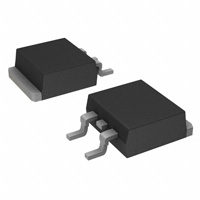
D2Pak IRG7S313UPbF
E Emitter
Description This IGBT is specifically designed for applications in Plasma Display Panels. This device utilizes advanced trench IGBT technology to achieve low VCE(on) and low EPULSETM rating per silicon area which improve panel efficiency. Additional features are 150°C operating junction temperature and high repetitive peak current capability. These features combine to make this IGBT a highly efficient, robust and reliable device for PDP applications.
Absolute Maximum Ratings
Parameter
VGE IC @ TC = 25°C IC @ TC = 100°C IRP @ TC = 25°C PD @TC = 25°C PD @TC = 100°C TJ TSTG Gate-to-Emitter Voltage Continuous Collector Current, VGE @ 15V Continuous Collector, VGE @ 15V Repetitive Peak Current Power Dissipation Power Dissipation Linear Derating Factor Operating Junction and Storage Temperature Range Soldering Temperature for 10 seconds 300
Max.
±30 40 20 160 78 31 0.63 -40 to + 150
Units
V A W W/°C °C
c
Thermal Resistance
RθJC Junction-to-Case
d
Parameter
Typ.
–––
Max.
1.6
Units
°C/W
www.irf.com
1
9/11/09
�IRG7S313UPbF
Electrical Characteristics @ TJ = 25°C (unless otherwise specified)
Parameter
BVCES ΔΒVCES/ΔTJ Collector-to-Emitter Breakdown Voltage Breakdown Voltage Temp. Coefficient
Min. Typ. Max. Units
330 ––– ––– ––– ––– 0.4 1.21 1.35 1.75 ––– ––– 2.14 1.41 ––– -10 1.0 25 ––– 75 ––– ––– 47 33 12 1.0 13 65 68 11 14 86 190 ––– 480 570 ––– ––– 1.45 ––– ––– ––– ––– 4.7 10 150 ––– 100 -100 ––– ––– ––– ––– ––– ––– ––– ––– ––– ––– ––– ––– ––– ––– ns μJ ns ns S nC nA μA V ––– mV/°C V
Conditions
VGE = 0V, ICE = 250μA
V V/°C Reference to 25°C, ICE = 1mA VGE = 15V, ICE = 12A VGE = 15V, ICE = 20A VGE = 15V, ICE VGE = 15V, ICE
VCE(on)
Static Collector-to-Emitter Voltage
VGE = 15V, ICE = 20A, TJ = 150°C VCE = VGE, ICE = 1.0mA VCE = 330V, VGE = 0V
e e = 40A e = 60A e
e
VGE(th) ΔVGE(th)/ΔTJ ICES
Gate Threshold Voltage Gate Threshold Voltage Coefficient Collector-to-Emitter Leakage Current
2.2 ––– –––
VCE = 330V, VGE = 0V, TJ = 125°C VCE = 330V, VGE = 0V, TJ = 150°C VGE = 30V VGE = -30V VCE = 25V, ICE = 12A VCE = 240V, IC = 12A, VGE = 15V IC = 12A, VCC = 196V RG = 10Ω , L=210μH TJ = 25°C IC = 12A, VCC = 196V RG = 10Ω , L=200μH, LS= 150nH TJ = 150°C VCC = 240V, VGE = 15V, RG= 5.1Ω L = 220nH, C= 0.20μF, VGE = 15V VCC = 240V, RG= 5.1Ω, TJ = 25°C L = 220nH, C= 0.20μF, VGE = 15V
IGES gfe Qg Qgc td(on) tr td(off) tf td(on) tr td(off) tf tst EPULSE
Gate-to-Emitter Forward Leakage Gate-to-Emitter Reverse Leakage Forward Transconductance Total Gate Charge Gate-to-Collector Charge Turn-On delay time Rise time Turn-Off delay time Fall time Turn-On delay time Rise time Turn-Off delay time Fall time Shoot Through Blocking Time Energy per Pulse
––– ––– ––– ––– ––– ––– ––– ––– ––– ––– ––– ––– ––– 100 ––– –––
e
Human Body Model ESD Machine Model Cies Coes Cres LC LE Input Capacitance Output Capacitance Reverse Transfer Capacitance Internal Collector Inductance Internal Emitter Inductance ––– ––– ––– ––– –––
VCC = 240V, RG= 5.1Ω, TJ = 100°C Class 1C (Per JEDEC standard JESD22-A114) Class B (Per EIA/JEDEC standard EIA/JESD22-A115) VGE = 0V 880 ––– 47 26 4.5 7.5 ––– ––– ––– nH ––– pF VCE = 30V ƒ = 1.0MHz Between lead, 6mm (0.25in.) from package and center of die contact
Notes: Half sine wave with duty cycle = 0.05, ton=2μsec. Rθ is measured at TJ of approximately 90°C. Pulse width ≤ 400μs; duty cycle ≤ 2%.
2
www.irf.com
�IRG7S313UPbF
200 VGE = 18V VGE = 15V VGE = 12V VGE = 10V 200 VGE = 18V VGE = 15V VGE = 12V VGE = 10V 160 160
ICE (A)
80
ICE (A)
120
VGE = 8.0V VGE = 6.0V
120
VGE = 8.0V VGE = 6.0V
80
40
40
0 0 2 4 6 VCE (V) 8 10
0 0 2 4 6 VCE (V) 8 10
Fig 1. Typical Output Characteristics @ 25°C
200 VGE = 18V VGE = 15V VGE = 12V VGE = 10V
Fig 2. Typical Output Characteristics @ 75°C
200 VGE = 18V VGE = 15V VGE = 12V VGE = 10V
160
160
ICE (A)
80
ICE (A)
120
VGE = 8.0V VGE = 6.0V
120
VGE = 8.0V VGE = 6.0V
80
40
40
0 0 2 4 6 VCE (V) 8 10
0 0 2 4 6 VCE (V) 8 10
Fig 3. Typical Output Characteristics @ 125°C
200
Fig 4. Typical Output Characteristics @ 150°C
14 IC = 12A 12 10
VCE (V)
160
ICE (A)
120 T J = 25°C 80
8 6 4
TJ = 25°C TJ = 150°C
T J = 150°C
40
2 0
2 4 6 8 10 12 14 16
0 V GE (V)
0
5
10 V GE (V)
15
20
Fig 5. Typical Transfer Characteristics
Fig 6. VCE(ON) vs. Gate Voltage
www.irf.com
3
�IRG7S313UPbF
50
200
Repetitive Peak Current (A)
40
160
30
IC (A)
120
20
80 ton= 2μs Duty cycle = 0.05 Half Sine Wave
10
40
0 0 25 50 75 TC (°C) 100 125 150
0 25 50 75 100 125 150 Case Temperature (°C)
Fig 7. Maximum Collector Current vs. Case Temperature
1300 1200 VCC = 240V L = 220nH C = variable 100°C
Fig 8. Typical Repetitive Peak Current vs. Case Temperature
1300 1200 L = 220nH C = 0.4μF 100°C
Energy per Pulse (μJ)
1100 1000 900 800 700 600 500 400
Energy per Pulse (μJ)
1100 1000 900 800 700 600
25°C
25°C
160
170
180
190
200
210
220
230
195 200 205 210 215 220 225 230 235 240 VCC, Collector-to-Supply Voltage (V)
IC, Peak Collector Current (A)
Fig 9. Typical EPULSE vs. Collector Current
1600 VCC = 240V 1400
Energy per Pulse (μJ)
Fig 10. Typical EPULSE vs. Collector-to-Supply Voltage
100
L = 220nH t = 1μs half sine
C= 0.4μF
10 μs 10
IC (A)
1200 1000 800 600 400 25 50 75 100 125 150 TJ, Temperature (ºC) C= 0.2μF
100 μs
C= 0.3μF
1ms 1
0.1 1 10 V CE (V) 100 1000
Fig 11. EPULSE vs. Temperature
Fig 12. Forrward Bias Safe Operating Area
4
www.irf.com
�IRG7S313UPbF
10000
20
VGE, Gate-to-Source Voltage (V)
ID= 12A VDS = 240V VDS = 150V VDS = 60V
16
Capacitance (pF)
1000
Cies
12
8
100
Coes Cres
10 0 100 200
4
0 0 10 20 30 40 QG Total Gate Charge (nC)
VCE (V)
Fig 13. Typical Capacitance vs. Collector-to-Emitter Voltage
Fig 14. Typical Gate Charge vs. Gate-to-Emitter Voltage
10
Thermal Response ( ZthJC )
1
D = 0.50 0.20
0.1
0.10 0.05 0.02 0.01
τJ τJ τ1
R1 R1 τ2
R2 R2
R3 R3 τ3
R4 R4 τC τ
τ1
τ2
τ3
τ4
τ4
0.01
Ci= τi/Ri Ci i /Ri
Ri (°C/W) τι (sec) 0.018158 0.000006 0.557463 0.00017 0.666413 0.001311 0.305061 0.006923
SINGLE PULSE ( THERMAL RESPONSE )
0.001 1E-006 1E-005 0.0001 0.001
Notes: 1. Duty Factor D = t1/t2 2. Peak Tj = P dm x Zthjc + Tc
0.01 0.1
t1 , Rectangular Pulse Duration (sec)
Fig 15. Maximum Effective Transient Thermal Impedance, Junction-to-Case
www.irf.com
5
�IRG7S313UPbF
A
RG
DRIVER L
C
PULSE A
VCC
B
PULSE B
RG
Ipulse DUT
tST
Fig 16a. tst and EPULSE Test Circuit
Fig 16b. tst Test Waveforms
VCE
Energy IC Current
0
L DUT 1K VCC
Fig 16c. EPULSE Test Waveforms
Fig. 17 - Gate Charge Circuit (turn-off)
6
www.irf.com
�IRG7S313UPbF
D2Pak (TO-263AB) Package Outline
Dimensions are shown in millimeters (inches)
D2Pak (TO-263AB) Part Marking Information
T HIS IS AN IRF530S WIT H LOT CODE 8024 AS S EMBLED ON WW 02, 2000 IN T HE AS S EMBLY LINE "L" INT ERNAT IONAL RECT IFIER LOGO AS S EMBLY LOT CODE PART NUMBER F530S DAT E CODE YEAR 0 = 2000 WEEK 02 LINE L
OR
INT ERNAT IONAL RECT IF IER LOGO AS SEMBLY LOT CODE PART NUMBER F 530S DAT E CODE P = DES IGNAT ES LEAD - F REE PRODUCT (OPT IONAL) YEAR 0 = 2000 WEEK 02 A = AS SEMBLY S IT E CODE
Note: For the most current drawing please refer to IR website at http://www.irf.com/package/
www.irf.com
7
�IRG7S313UPbF
D2Pak (TO-263AB) Tape & Reel Information
Dimensions are shown in millimeters (inches)
TRR
1.60 (.063) 1.50 (.059) 4.10 (.161) 3.90 (.153)
1.60 (.063) 1.50 (.059)
0.368 (.0145) 0.342 (.0135)
FEED DIRECTION 1.85 (.073)
1.65 (.065)
11.60 (.457) 11.40 (.449)
15.42 (.609) 15.22 (.601)
24.30 (.957) 23.90 (.941)
TRL
10.90 (.429) 10.70 (.421) 1.75 (.069) 1.25 (.049) 16.10 (.634) 15.90 (.626) 4.72 (.136) 4.52 (.178)
FEED DIRECTION
13.50 (.532) 12.80 (.504)
27.40 (1.079) 23.90 (.941)
4
330.00 (14.173) MAX.
60.00 (2.362) MIN.
NOTES : 1. COMFORMS TO EIA-418. 2. CONTROLLING DIMENSION: MILLIMETER. 3. DIMENSION MEASURED @ HUB. 4. INCLUDES FLANGE DISTORTION @ OUTER EDGE.
26.40 (1.039) 24.40 (.961) 3
30.40 (1.197) MAX. 4
Note: For the most current drawing please refer to IR website at http://www.irf.com/package/ Data and specifications subject to change without notice. This product has been designed for the Industrial market. Qualification Standards can be found on IR’s Web site.
IR WORLD HEADQUARTERS: 233 Kansas St., El Segundo, California 90245, USA Tel: (310) 252-7105 TAC Fax: (310) 252-7903 Visit us at www.irf.com for sales contact information.09/2009
8
www.irf.com
�