IRGI4086PbF
PDP TRENCH IGBT
Features Advanced Trench IGBT Technology l Optimized for Sustain and Energy Recovery Circuits in PDP Applications TM) l Low VCE(on) and Energy per Pulse (EPULSE for Improved Panel Efficiency l High Repetitive Peak Current Capability l Lead Free Package
l
PD - 96223
Key Parameters
VCE min VCE(ON) typ. @ IC = 25A IRP max @ TC= 25°C TJ max
C
c
300 1.29 230 150
V V A °C
G E
E C G
n-channel
G G ate C C ollector
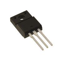
TO-220AB Full-Pak
E E m itter
Description This IGBT is specifically designed for applications in Plasma Display Panels. This device utilizes advanced trench IGBT technology to achieve low VCE(on) and low EPULSETM rating per silicon area which improve panel efficiency. Additional features are 150°C operating junction temperature and high repetitive peak current capability. These features combine to make this IGBT a highly efficient, robust and reliable device for PDP applications.
Absolute Maximum Ratings
Parameter
VGE IC @ TC = 25°C IC @ TC = 100°C IRP @ TC = 25°C PD @TC = 25°C PD @TC = 100°C TJ TSTG Gate-to-Emitter Voltage Continuous Collector Current, VGE @ 15V Continuous Collector, VGE @ 15V Repetitive Peak Current Power Dissipation Power Dissipation Linear Derating Factor Operating Junction and Storage Temperature Range Soldering Temperature for 10 seconds Mounting Torque, 6-32 or M3 Screw
Max.
±30 25 12 230 43 17 0.34 -40 to + 150 300
Units
V A
c
W W/°C °C
10lb in (1.1N m)
x
x
N
Thermal Resistance
RθJC Junction-to-Case
d
Parameter
Typ.
–––
Max.
2.9
Units
°C/W
www.irf.com
1
02/02/09
�IRGI4086PbF
Electrical Characteristics @ TJ = 25°C (unless otherwise specified)
Parameter
Collector-to-Emitter Breakdown Voltage ∆ΒVCES/∆TJ Breakdown Voltage Temp. Coefficient BVCES
Min.
300 ––– ––– ––– ––– ––– ––– ––– 2.6 ––– ––– ––– ––– ––– ––– ––– ––– ––– — — — — — — — — 100 ––– –––
Typ. Max. Units
––– 0.29 1.10 1.29 1.49 1.90 2.57 2.27 ––– -11 2.0 5.0 100 ––– ––– 29 65 22 36 31 112 65 30 33 145 98 ––– 1075 1432 2250 110 58 5.0 13
Conditions
VCE(on)
Static Collector-to-Emitter Voltage
VGE(th) ∆VGE(th)/∆TJ ICES
Gate Threshold Voltage Gate Threshold Voltage Coefficient Collector-to-Emitter Leakage Current
IGES gfe Qg Qgc td(on) tr td(off) tf td(on) tr td(off) tf tst EPULSE
Gate-to-Emitter Forward Leakage Gate-to-Emitter Reverse Leakage Forward Transconductance Total Gate Charge Gate-to-Collector Charge Turn-On delay time Rise time Turn-Off delay time Fall time Turn-On delay time Rise time Turn-Off delay time Fall time Shoot Through Blocking Time Energy per Pulse
Ciss Coss Crss LC LE
Input Capacitance Output Capacitance Reverse Transfer Capacitance Internal Collector Inductance Internal Emitter Inductance
––– ––– ––– ––– –––
––– V VGE = 0V, ICE = 1 mA ––– V/°C Reference to 25°C, ICE = 1mA VGE = 15V, ICE = 12A 1.36 VGE = 15V, ICE = 25A 1.55 VGE = 15V, ICE = 40A 1.67 V VGE = 15V, ICE = 70A 2.10 VGE = 15V, ICE = 120A 2.96 VGE = 15V, ICE = 70A, TJ = 150°C ––– 5.0 V VCE = VGE, ICE = 500µA ––– mV/°C 25 µA VCE = 300V, VGE = 0V VCE = 300V, VGE = 0V, TJ = 100°C ––– VCE = 300V, VGE = 0V, TJ = 150°C ––– 100 nA VGE = 30V VGE = -30V -100 ––– S VCE = 25V, ICE = 25A ––– nC VCE = 200V, IC = 25A, VGE = 15V ––– IC = 25A, VCC = 196V — — ns RG = 10Ω, L=200µH, LS= 200nH TJ = 25°C — — IC = 25A, VCC = 196V — — ns RG = 10Ω, L=200µH, LS= 200nH TJ = 150°C — — ––– ns VCC = 240V, VGE = 15V, RG= 5.1Ω L = 220nH, C= 0.40µF, VGE = 15V ––– µJ VCC = 240V, RG= 5.1Ω, TJ = 25°C L = 220nH, C= 0.40µF, VGE = 15V ––– VCC = 240V, RG= 5.1Ω, TJ = 100°C VGE = 0V ––– ––– pF VCE = 30V
e e e e e
e
––– ––– nH –––
ƒ = 1.0MHz,
See Fig.13
Between lead, 6mm (0.25in.) from package and center of die contact
Notes: Half sine wave with duty cycle = 0.1, ton=2µsec. Rθ is measured at TJ of approximately 90°C.
Pulse width ≤ 400µs; duty cycle ≤ 2%.
2
www.irf.com
�IRGI4086PbF
240 200 160
ICE (A)
240 VGE = 18V VGE = 15V VGE = 12V VGE = 10V 200 160
ICE (A)
120 80 40 0 0 4 8 VCE (V)
VGE = 8.0V VGE = 6.0V
VGE = 18V VGE = 15V VGE = 12V VGE = 10V
120 80 40 0
VGE = 8.0V VGE = 6.0V
12
16
0
4
8 VCE (V)
12
16
Fig 1. Typical Output Characteristics @ 25°C
240 200 160
ICE (A)
Fig 2. Typical Output Characteristics @ 75°C
240 200 160
ICE (A)
VGE = 18V VGE = 15V VGE = 12V VGE = 10V
120 80 40 0 0 4 8 VCE (V)
VGE = 8.0V VGE = 6.0V
VGE = 18V VGE = 15V VGE = 12V VGE = 10V
120 80 40 0
VGE = 8.0V VGE = 6.0V
12
16
0
4
8 VCE (V)
12
16
Fig 3. Typical Output Characteristics @ 125°C
240 200 T J = 25°C 160 T J = 150°C
Fig 4. Typical Output Characteristics @ 150°C
10 IC = 25A 8
120 80 40 0 2 4 6 8 10 12 14 16 VGE (V)
VCE (V)
ICE (A)
6
TJ = 25°C TJ = 150°C
4
2
0 5 10 V GE (V) 15 20
Fig 5. Typical Transfer Characteristics
Fig 6. VCE(ON) vs. Gate Voltage
www.irf.com
3
�IRGI4086PbF
30 25
240 220 200
Repetitive Peak Current (A)
ton= 2µs Duty cycle
很抱歉,暂时无法提供与“IRGI4086PBF”相匹配的价格&库存,您可以联系我们找货
免费人工找货