PD-95882
IRGP4050
PDP Switch
Features
§ § § §
§ §
Key parameters optimized for PDP sustain & Energy recovery applications 104A continuous collector current rating reduces component count High pulse current rating makes it ideal for capacitive load circuits Low temperature co-efficient of VCE (ON) ensures reduced power dissipation at operating junction temperatures Reverse voltage avalanche rating improves the robustness in sustain driver application Short fall & rise times for fast switching
C
VCES = 250V
G E
VCE(on) typ. = 1.64V
@VGE = 15V, IC = 30A
n-channel
Description
This IGBT is specifically designed for sustain & energy recovery application in plasma display panels. This IGBT features low V CE (ON) and fast switching times to improve circuit efficiency and reliability. Low temperature co-efficient of VCE (ON) makes this IGBT an ideal device for PDP sustain driver application.
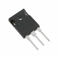
TO-247AC
Absolute Maximum Ratings
Parameter
VCES IC @ TC = 25°C IC @ TC = 100°C ICM ILM VGE EARV PD @ TC = 25°C PD @ TC = 100°C TJ TSTG Collector-to-Emitter Voltage Continuous Collector Current Continuous Collector Current Pulse Collector Current Clamped Inductive Load current
Max.
250 104* 56 208 290 ±20 1240 330 130 -55 to +150 300 (0.063 in. (1.6mm) from case)
Units
V A
Ã
Gate-to-Emitter Voltage Reverse Voltage Avalanche Energy
d
Maximum Power Dissipation Maximum Power Dissipation Operating Junction and Storage Temperature Range Solder Temperature Range, for 10 sec.
e
V mJ W
°C
Thermal / Mechanical Characteristics
Parameter
RθJC RθCS RθJA Wt Junction-to-Case- IGBT Case-to-Sink, flat, greased surface Junction-to-Ambient, typical socket mount Weight
Min.
––– ––– ––– –––
Typ.
––– 0.24 ––– 6 (0.21)
Max.
0.38 ––– 40 –––
Units
°C/W
g (oz.)
*Package limited to 60A.
1
www.irf.com
07/05/04
�IRGP4050
Electrical Characteristics @ TJ = 25°C (unless otherwise specified)
Parameter
Collector-to-Emitter Breakdown Voltage V(BR)CES V(BR)ECS Emitter-to-Collector Breakdown Voltage ∆V(BR)CES/∆TJ Temperature Coeff. of Breakdown Voltage
Min. Typ. Max. Units
Conditions
fÃ
VCE(on) VGE(th) ∆VGE(th)/∆TJ gfe ICES
Collector-to-Emitter Saturation Voltage Gate Threshold Voltage Threshold Voltage temp. coefficient Forward Transconductance Zero Gate Voltage Collector Current
gÃ
IGES
Gate-to-Emitter Leakage Current
250 18 — — — — 3.0 — 34 — — — —
— — V VGE = 0V, IC = 250µA — — V VGE = 0V, IC = 1.0A 8.2 — mV/°C VGE = 0V, IC = 1mA IC = 30A 1.64 1.90 IC = 56A VGE = 15V 2.04 — V IC = 104A, TJ = 150°C See Fig. 2, 5 2.60 — VCE = VGE, IC = 250µA — 6.0 -11 — mV/°C VCE = VGE, IC = 0.25mA 51 — S VCE = 100V, IC = 56A VGE = 0V, VCE = 250V — 250 — 2.0 µA VGE = 0V, VCE = 10V VGE = 0V, VCE = 250V, TJ = 150°C — 5000 — ±100 nA VGE = ±20V
Switching Characteristics @ TJ = 25°C (unless otherwise specified)
Parameter
Qg Qge Qgc td(on) tr td(off) tf Eon Eoff ETS td(on) tr td(off) tf ETS LE Cies Coes Cres
Notes:
Min. Typ. Max. Units
— — — — — — — — — — — — — — — — — — — 230 37 78 37 35 120 59 45 125 170 35 35 130 120 280 13 4650 480 92 350 56 120 — — 180 89 — — — — — — — — — — — — nC
Conditions
IC = 56A VCC = 200V See Fig. 8 VGE = 15V TJ = 25°C IC = 30A, VCC = 180V VGE = 15V, RG = 5.0Ω Energy losses include "tail" See Fig. 9, 10, 14
Total Gate Charge (turn-on) Gate-to-Emitter Charge (turn-on) Gate-to-Collector Charge (turn-on) Turn-On delay time Rise time Turn-Off delay time Fall time Turn-On Switching Loss Turn-Off Switching Loss Total Switching Loss Turn-On delay time Rise time Turn-Off delay time Fall time Total Switching Loss Internal Emitter Inductance Input Capacitance Output Capacitance Reverse Transfer Capacitance
ns
µJ TJ = 150°C IC = 30A, VCC = 180V VGE = 15V, RG = 5.0Ω Energy losses include "tail" See Fig. 11, 14 Measured 5mm from package VGE = 0V VCC = 30V, See Fig. 7 f = 1.0MHz
ns
µJ nH pF
Repetitive rating; VGE = 20V, pulse width limited by max. junction temperature. ( See fig. 13b ) VCC = 80%(VCES ), VGE = 20V, L = 10µH, RG = 5.0Ω, (See fig. 13a). Repetitive rating; pulse width limited by maximum junction temperature. Pulse width ≤ 2.5ms; duty factor ≤ 0.1%. Pulse width 5.0µs, single shot.
2
www.irf.com
�IRGP4050
140
Triangular wave:
120 100
Clamp voltage: 80% of rated
Load Current ( A )
For both: Duty cycle : 50% Tj = 125°C Tsink = 90°C Gate drive as specified Power Dissipation = 73W
80 60
Square wave: 60% of rated voltage
40 20 0 0.1
Ideal diodes
1
10
100
f , Frequency ( kHz )
Fig. 1 - Typical Load Current vs. Frequency
(Load Current = IRMS of fundamental)
1000
IC, Collector-to-Emitter Current (A)
1000
IC, Collector-to-Emitter Current (A)
100
T J = 150°C
100
10 T J = 150°C 1 TJ = 25°C
10
1
T J = 25°C
0.1
V GE = 15V 20µs PULSE WIDTH
0.1 0.1 1 10 100 V CE, Collecto-to-Emitter Voltage (V)
VCC = 50V 20µs PULSE WIDTH 0 2 4 6 8 10 12 14 16
0.01 VGE, Gate-to-Emitter Voltage (V)
Fig. 2 - Typical Output Characteristics
Fig. 3 - Typical Transfer Characteristics
www.irf.com
3
�IRGP4050
120
4.0
100
VCE , Collector-to Emitter Voltage (V)
Maximum DC Collector Current (A)
LIMITED BY PACKAGE
VGE = 15V 80µs PULSE WIDTH
80
3.0
IC = 112A
60
IC = 56A
2.0
40
IC = 28A
20
0 25 50 75 100 125 150
1.0 -60 -40 -20 0 20 40 60 80 100 120 140 160
T C , Case Temperature (°C)
T J , Junction Temperature (°C)
Fig. 4 - Maximum Collector Current vs. Case Temperature
Fig. 5 - Typical Collector-to-Emitter Voltage vs. Junction Temperature
1
Thermal Response ( Z thJC )
D = 0.50
0.1
0.20 0.10 0.05
R1 R1 τJ τ1 τ2 R2 R2 R3 R3 τ3 τC τ τ3
0.01
0.02 0.01
τJ
τ1
τ2
Ri (°C/W) τi (sec) 0.0906 0.000350 0.0906 0.002209 0.2003 0.028536
0.001
Ci= τi /Ri Ci i/Ri
SINGLE PULSE ( THERMAL RESPONSE )
Notes: 1. Duty Factor D = t1/t2 2. Peak Tj = P dm x Zthjc + Tc
0.001 0.01 0.1 1
0.0001 1E-006 1E-005 0.0001
t1 , Rectangular Pulse Duration (sec)
Fig. 6 - Maximum Effective Transient Thermal Impedance, Junction-to-Case
4
www.irf.com
�IRGP4050
100000 VGS = 0V, f = 1 MHZ C ies = C ge + C gd, C ce SHORTED C res = C gc C oes = C ce + Cgc
16 14 12 10 8 6 4 2 0
VCES = 200V IC = 56A
10000
Cies
1000
Coes
100
Cres
10 0 50 100 150 200
VGE, Gate-to-Emitter Voltage (V)
Capacitance (pF)
0
50
100
150
200
VCE, Collector-toEmitter-Voltage(V)
Q G, Total Gate Charge (nC)
Fig. 7 - Typical Capacitance vs. Collector-to-Emitter Voltage
Fig. 8 - Typical Gate Charge vs. Gate-to-Emitter Voltage
2400 2200 VCE = 200V VGE = 15V
7000 6000
Total Swiching Losses (µJ)
2000 1800 1600 1400 1200 1000 800 0
Total Swiching Losses (µJ)
TJ = 25°C I C = 56A
RG = 5.0Ω V GE = 15V
Ã
IC = 112A
5000 4000 3000 2000 1000 0
IC = 56A IC = 28A
-55 -5 45 95 145
5
10
15
20
25
30
RG, Gate Resistance (Ω)
T J, Juntion Temperature (°C)
Fig. 9 - Typical Switching Losses vs. Gate Resistance
Fig. 10 - Typical Switching Losses vs. Junction Temperature
www.irf.com
5
�IRGP4050
6000
1000
5000
V CE= 200V
4000
V GE = 15V
IC, Collector-to-Emitter Current (A)
RG = 5.0Ω TJ = 150°C
VGE = 20V T J = 125°
100
Total Swiching Losses (µJ)
3000
2000
10
SAFE OPERATING AREA
1000
0 20 40 60 80 100 120
1 1 10 100 1000
IC, Collecto-to-Emitter (A)
VDS, Drain-to-Source Voltage (V)
Fig. 11 - Typical Switching Losses vs. Collector-to-Emitter Current
Fig. 12 - Turn-Off SOA
6
www.irf.com
�IRGP4050
L 50V 1000V VC *
0 - 480V
D.U.T.
RL =
480V 4 X I C@25°C
c
480µF 960V
d
* Driver same type as D.U.T.; Vc = 80% of Vce(max) * Note: Due to the 50V power supply, pulse width and inductor will increase to obtain rated Id.
Fig. 13a - Clamped Inductive
Load Test Circuit
Fig. 13b - Pulsed Collector
Current Test Circuit
IC L Driver* 50V 1000V VC D.U.T.
Fig. 14a - Switching Loss
Test Circuit
* Driver same type as D.U.T., VC = 480V
Ã
d
e
c d
90%
e
VC 90%
10%
t d(off)
Fig. 14b - Switching Loss
Waveforms
10% I C 5% t d(on)
tr E on E ts = (Eon +Eoff )
tf t=5µs E off
www.irf.com
7
�IRGP4050
TO-247AC Package Outline
Dimensions are shown in millimeters (inches)
TO-247AC Part Marking Information
@Y6HQG@) UCDTÃDTÃ6IÃDSAQ@"�à XDUCÃ6TT@H7G`à GPUÃ8P9@Ã$%$& 6TT@H7G@9ÃPIÃXXÃ"$�Ã!��� DIÃUC@Ã6TT@H7G`ÃGDI@ÃÅCÅ
Note: "P" in assembly line position indicates "Lead-Free"
DIU@SI6UDPI6G S@8UDAD@S GPBP 6TT@H7G` GPUÃ8P9@
Q6SUÃIVH7@S
,5)3(��
Ã�"$C $%ÃÃÃÃÃÃÃÃÃÃÃ$&
96U@Ã8P9@ `@6SÃ�Ã2Ã!��� X@@FÃ"$ GDI@ÃC
TO-247AC
package is not recommended for Surface Mount Application.
Data and specifications subject to change without notice. This product has been designed and qualified for the Industrial market. Qualification Standards can be found on IR’s Web site.
IR WORLD HEADQUARTERS: 233 Kansas St., El Segundo, California 90245, USA Tel: (310) 252-7105 TAC Fax: (310) 252-7903 Visit us at www.irf.com for sales contact information.06/04
8
www.irf.com
�