Data SheetNo. PD60188-B
IRIS4011(K)
INTEGRATED SWITCHER
Features
• Primary current mode control, and secondary
voltage mode control • Vcc Over-voltage protection (latched) • Over-current & over-temperature protection • Quasi resonant, variable frequency operation • 5 pin TO-220 and TO-262 • 3.9Ω Rds(on) max/ 650V MOSFET • Fully Characterized Avalanche Energy
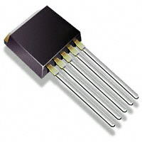
IRIS4011 5 Lead TO-220 IRIS4011K 5 Lead TO-262
Packages
Description
The IRIS4011(K) is a dual mode voltage and current controller combined with a MOSFET in a single package. The IRIS4011(K) is designed for use in universal and single input AC/DC and DC/DC switching power supplies and is capable of powers up to 60W for a universal line input. The device can operate in either a quasi-resonant or Pulse Ratio Control (PRC) mode, and thereby variable frequency operation.
Typical Connection Diagram
Vin (AC/ DC)
Vout (DC)
3
Drain Vcc
4
IRIS4011(K)
FB Source Gnd
5
1
2
(Refer to Lead Assignments for correct pin configuration). This/These diagram(s) show electrical connections only. Please refer to our DesignTips and Application Notes (AN1018a, AN1024a, AN1025) for proper circuit board layout.
www.irf.com
1
�IRIS4011(K)
Absolute Maximum Ratings
Absolute maximum ratings indicate sustained limits beyond which damage to the device may occur. All voltage parameters are absolute voltages referenced to terminals stated, all currents are defined positive into any lead. The thermal resistance and power dissipation ratings are measured under board mounted and still air conditions.
Symbol
IDpeak IDmax EAS VCC VTH P D1 P D2 RthJC TJ TS Tf TOP TL
Definition
Peak drain current Maximum switching current Single pulse avalanche energy Power supply voltage OCP/FB terminal voltage Power dissipation for MOSFET Power dissipation for control part (MIC) Thermal resistance, junction to case Junction temperature Storage temperature Internal frame temperature in operation Ambient operating temperature Lead temp. (soldering, 10 seconds)
Terminals
3-1 3-1 3-1 4-3 5-2 3-1 4-2 — — — — — —
Max. Ratings
6.8 2.7 92 35 6 89 1.4 0.8 1.4 -40-125 -40-125 -20-125 -20-125 300
Units
A mJ
Note
Single pulse V2-3 = 0.78V Tc=25oC Vdd=99V,L=20mH, G=12V, Ipk=2.8A
V With infinite heatsink W Without heatsink Specified by VIN x IIN °C/W
°C
Refer to recommended operating temperature
Recommended Operating Conditions
Time for input of quasi resonant signals. For the Quasi resonant signal inputted to the VDCP/FB terminal at the time of quasi resonant operation, the signal should be wider thant Tth(2)
VOCP/FB Tth(2) ≥1.0µs Vth(2)
2
www.irf.com
�IRIS4011(K)
Electrical Characteristics (for Control IC)
VCC = 18V, (TA = 25 °C) unless otherwise specified.
Symbol
VCCUV+ VCCUVIQCCUV IQCC TOFF/(MAX) TTH(2) TOFF/(MIN) VTH(1) VTH(2) IOCP/FB VCC(OVP) ICC(LA) VCC(LaOFF) TJ(TSD)
Definition
VCC supply undervoltage positive going threshold VCC supply undervoltage negative going threshold UVLO mode quiescent current Quiescent operating VCC supply current Maximum OFF time Minimum input pulse width for quasi resonant signals Minimum OFF time OCP/FB terminal threshold voltage 1 OCP/FB terminal threshold voltage 2 OCP/FB terminal sink current VCC overvoltage protection limit Latch circuit holding current Latch circuit reset voltage Thermal shutdown activation temperature
Min. Typ. Max. Units Test Conditions
14.4 9 — — 40 — — 0.68 1.3 1.1 20.5 — 6.6 140 16 10 — — — — — 0.73 1.45 1.35 22.5 — — — 17.6 11 100 30 60 1.0 1.5 0.78 1.6 1.7 24.5 400 8.4 — V mA V µA V
oC
V µA mA µsec VCC < VCCUV+
Electrical Characteristics (for MOSFET)
(TA = 25°C) unless otherwise specified.
Symbol
VDSS IDSS RDS(ON) tr
THj-C
Definition
Drain-to-source breakdown voltage Drain leakage current On-resistance Rise time (10% to 90%) Thermal resistance
Min. Typ. Max. Units Test Conditions
650 — — — — — — — — — — 300 3.9 250 1.4 V µA Ω ns oC/W Vds=520V, VCC=0V Tj =125oC V3-1=10V, ID=0.9A Between junction and case
www.irf.com
3
�IRIS4011(K)
Block Diagram
4 Vcc
3 START O.V.P LATCH D
REG.
DRIVE 1
T.S.D OSCILLATOR
S Vth(1) 5 OCP/ FB
+
Comp.1
+
Comp.2
Vth(2)
2 Ground
Lead Assignments
Pin # S y m b o l
1 S
Description
MOSFET Source terminal
2
Ground
Ground terminal
3
D
MOSFET Drain terminal
4 1 2 3 4 5 5
Vcc
Control circuit supply volta g e
OCP/FB
Overcurrent detection, and Volta g e mode control feedback si g nal
Other Functions
O.V.P. – Overvoltage Protection Circuit T.S.D. – Thermal Shutdown Circuit 4 www.irf.com
�IRIS4011(K)
Case outline
5-Lead TO-220
01-6020 00 01-3042 01 (TS-001)
www.irf.com
5
�IRIS4011(K)
Case outline
1.40 [.055] MAX. 10.29 [.405] 9.65 [.380] 4.83 [.190] 4.06 [.160] B 1.32 [.052] 1.22 [.048] 6.22[.245] MIN
6
9.65 [.380] 8.64 [.340]
6
8.00[.315] MAX
12345
C 12.70 [.500] 14.73 [.580]
5X 1.70 [.067] 4X
1.01[.040] 0.51[.020] A B
5X
0.63 [.025] 0.31 [.012] 2.92 [.115] 2.16 [.085]
0.25 [.010]
5-Lead TO-262
IR WORLD HEADQUARTERS: 233 Kansas Street, El Segundo, California 90245 Tel: (310) 252-7105 Data and specifications subject to change without notice. 10/162001
6
www.irf.com
�
很抱歉,暂时无法提供与“IRIS4011K”相匹配的价格&库存,您可以联系我们找货
免费人工找货