PD - 94804A
AUTOMOTIVE MOSFET
Features
l l l l l l
Logic Level Advanced Process Technology Ultra Low On-Resistance 175°C Operating Temperature Fast Switching Repetitive Avalanche Allowed up to Tjmax
G
HEXFET® Power MOSFET
D
IRL1404Z IRL1404ZS IRL1404ZL
VDSS = 40V
RDS(on) = 3.1mW ID = 75A
S
Description
Specifically designed for Automotive applications, this HEXFET® Power MOSFET utilizes the latest processing techniques to achieve extremely low on-resistance per silicon area. Additional features of this design are a 175°C junction operating temperature, fast switching speed and improved repetitive avalanche rating . These features combine to make this design an extremely efficient and reliable device for use in Automotive applications and a wide variety of other applications.
TO-220AB IRL1404Z
D2Pak IRL1404ZS
TO-262 IRL1404ZL
5h
xqÂGguyyÂRgus
8 7 8Â4ÂT7Â1Â���u7 C 8Â4ÂT7Â1 #u7 C 8G P 8Â4T 7Â1 #u7
C C Â4ÂT Â1Â #u7 V 9
2CTCOGVGT
Â4Â��VÂ�SuxuiÂFuyuqp�
/CZ�
�� �"� %# %'� !� ��#
7PKVU
5
AS ASÂ4Â��V 7u
Â8guÂ7q�ÂV ASÂ4Â��VÂ�PgiwgsqÂFuyuqp�
7u
Â8guÂ7q�ÂV 7u
Â8guÂ7q�ÂV Px
qpÂ8guÂ7q PqÂ8u
uguÂÂ FuqgÂ8qgusÂ@giÂÂ
W W�u7 V yD
AS
Agq��SiqÂVxgsq
5SÂ�TtqygxxÂxuyuqp� 5SÂ�Tq
qp� C 5R 9 5R
9 T T
SusxqÂPx
qÂ5gxgitqÂ9qs
d
ÂvÂ�$
SusxqÂPx
qÂ5gxgitqÂ9qsÂTq
qpÂVgxq 5gxgitqÂ7q
Ã
h
� "'� SqqÂ@us�� g�Â� h�Â�#�Â�$
RqquuqÂ5gxgitqÂ9qs IqgusÂDiuÂgp SgsqÂTqyqgqÂRgsq
DÂ STA
g
5 yD
�##ÂÂÂ�Â�%# u7 !��Â���$yyÂryÂig
qÂ� ��Âxhr uÂ����H y�
SxpqusÂTqyqgq�ÂrÂ��Â
qip
TtqygxÂRq
u
giq
D7Â RT7SÂ RTD5Â RTD5Â
RT
GusÂTq�Â$�! ÂÂG!Â
iq
y
y
2CTCOGVGT
6[R�
/CZ�
��$# $ "�
7PKVU
u7�W
Diu��7g
q 7g
q��Suw�Â@xg�ÂAqg
qpÂSrgiq Diu��5yhuqÂ
i
i
��#�
Diu��5yhuqÂ�P76ÂG�Â
jÃ
www.irf.com
1
2/2/04
�IRL1404Z/S/L
9xqiuigxÂ7tggiqu
ui
Â4ÂT,Â1 #u7Â�xq
Âtqu
qÂ
qiuruqp�
V 'V R
�6R�8SS �6R�8SS
�'T
DÂ
8S��
8gu��SiqÂ6qgwpÂVxgsq 6qgwpÂVxgsqÂTqy�Â7qrruiuq SguiÂ8gu��SiqÂI�Rq
u
giq AgqÂTtq
txpÂVxgsq @gpÂTg
ipigiq 8gu��SiqÂFqgwgsqÂ7q Agq��SiqÂ@gpÂFqgwgsq Agq��SiqÂRqq
qÂFqgwgsq TgxÂAgqÂ7tgsq Agq��SiqÂ7tgsq Agq��8guÂ�ÄGuxxqÄ�Â7tgsq T�IÂ8qxgÂTuyq Ru
qÂTuyq T�IrrÂ8qxgÂTuyq @gxxÂTuyq CqgxÂ8guÂCpigiq CqgxÂSiqÂCpigiq CÂ7ggiugiq IÂ7ggiugiq Rqq
qÂTg
rqÂ7ggiugiq IÂ7ggiugiq IÂ7ggiugiq 9rrqiuqÂIÂ7ggiugiq
Pggyqq
Gu� T� Gg� Uu
"� ���!" �# !�#
V sr
C C
AS�t�
��" ��
8SS
ASS
Q Q Q F
r
s s
sp
p��
p�rr�
8
%# & "� �' �&� !� "' "�# %�# #�&� '%� #%� !!�� &%� � &�
F
S
7 7 7 7 7 7 Âqrr�
u
Siq�8guÂRgus
ÂgpÂ7tggiqu
ui
ÂÂÂÂÂÂÂÂPggyqq
7u
ÂSiqÂ7q �6pÂ8upq� Px
qpÂSiqÂ7q �6pÂ8upq�à 8upqÂ@gpÂVxgsq Rqq
qÂRqiqÂTuyq Rqq
qÂRqiqÂ7tgsq @gpÂT�IÂTuyq
V V Â1Â�V�ÂC Â1 #�z5 V�u7 Rqrqqiq #u7�ÂC Â1Â�y5 !�� y: V Â1Â��V�ÂC Â1Â%#5Âe "�% V Â1Â#��V�ÂC Â1Â"�5Âe �% V V Â1ÂV �ÂC Â1 #�z5 S V Â1Â��V�ÂC Â1Â%#5 � z5 V Â1Â"�V�ÂV Â1Â�V #� V Â1Â"�V�ÂV Â1Â�V�ÂT Â1Â� #u7 �� 5 V Â1Â�$V � �� V Â1Â��$V ��� C Â1Â%#5 7 V Â1Â! V V Â1Â#��VÂe V Â1 �V C Â1Â%#5
R Â1Â"��: V Â1Â#��VÂe 6qqqÂxqgp� D B $yyÂ��� #u�� G ryÂgiwgsq S gpÂiqqÂrÂpuqÂigi V Â1Â�V V Â1 #V @ Â1Â���GB V Â1Â�V�ÂÂV Â1Â���V� Â1Â���GB V Â1Â�V�ÂÂV Â1Â! V� Â1Â���GB V Â1Â�V�ÂV Â1Â�VÂÂ! VÂf
AS 8 8 AS AS 8S 8S 8S 8S 8 8 AS 8 8 AS AS D AS AS 8 8S AS 88 8 A AS AS 8S AS AS AS 8S 8S 8S
7puu
C5 C5/ V5& TT QTT QP
Gu� T� Gg� Uu
�&� %� $ �& ��! !' %
GIS@9TÂ
yhx 5
tusÂÂtq uqsgxÂqq
q �ÂviuÂpupq� V T,Â1 #u7�ÂC5Â1Â%#5�ÂV)5Â1Â�VÂe
T,Â1 #u7�ÂC(Â1Â%#5�ÂV Â1 �V 7 pu�pÂ1Â���5�z
Âe
G
88
7puu
D
S
Cu
uiÂ�ÂuyqÂu
ÂqsxusuhxqÂ��Âu
ÂpyugqpÂhÂFS�F8�
Notes: Repetitive rating; pulse width limited by max. junction temperature. (See fig. 11). Limited by TJmax, starting TJ = 25°C, L = 0.079mH, RG = 25W, IAS = 75A, VGS =10V. Part not recommended for use above this value. Pulse width £ 1.0ms; duty cycle £ 2%. Coss eff. is a fixed capacitance that gives the same charging time as Coss while VDS is rising from 0 to 80% VDSS .
Limited by TJmax , see Fig.12a, 12b, 15, 16 for typical This value determined from sample failure population. 100% This is only applied to TO-220AB package. When mounted on 1" square PCB (FR-4 or G-10 Material).
For recommended footprint and soldering techniques refer to application note #AN-994. tested to this value in production. repetitive avalanche performance.
2
www.irf.com
�IRL1404Z/S/L
1000
TIPÂÂÂÂÂÂÂÂÂÂ
ID, Drain-to-Source Current (A)
100
6ITTIG
ID, Drain-to-Source Current (A)
VAS ��V %��V #��V "�#V "��V !�#V !�!V !��V
1000
TIP VAS ��V %��V #��V "�#V "��V !�#V !�!V !��V
100
6ITTIG
!��V
10
10
!��V
1 0.1 1
$�z
ÂPUFS9ÂWC8TB TvÂ1Â #u7
10 100 V DS, Drain-to-Source Voltage (V)
1 0.1 1
$�z
ÂPUFS9ÂWC8TB TvÂ1Â�%#u7
10 100
V DS, Drain-to-Source Voltage (V)
Fig 1. Typical Output Characteristics
Fig 2. Typical Output Characteristics
1000
��
$ �
�
T DÂ1Â�%#u7
100
 q 7  q i S � � u g 8  � 8 C
10
T DÂ1 #u7 V8SÂ1Â��V $�z
ÂPUFS9ÂWC8TB
2 3 4 5 6 7 8 9 10
� S � Âq i g i p i
g T Âp g @ �Â
r A
TDÂ1Â #u7 �#�
���
T DÂ1Â�%#u7
#�
V DS = 10V
1.0
�
�
#�
���
�#�
��
VAS�ÂAgq��SiqÂVxgsqÂ�V�
Fig 3. Typical Transfer Characteristics
C8�8gu��SiqÂ7qÂ�5�
Fig 4. Typical Forward Transconductance vs. Drain Current
www.irf.com
3
�IRL1404Z/S/L
$��
������
� @ ����� � q i g ui g g 7���� �Â7
VASÂÂÂ1Â�V�ÂÂÂÂÂÂÂrÂ1Â�ÂGB` 7u
 ÂÂ1Â7 s
 �Â7sp�ÂÂ7 p
 SBIRT98 7
 Â1Â7 sp 7
ÂÂ 1Â7p
 �Â7sp
7u
7
7
� V � Â q s g x V Â q i S � � q g A Â �S A V
���
C81Â%#5
#�� "�� !�� �� ��� ���
V8S1Â! V V8S1Â �V
��� � ��
�
�
"�
$�
&�
V8S�Â8gu��SiqÂVxgsqÂ�V�
Fig 5. Typical Capacitance vs. Drain-to-Source Voltage
ÂQAÂÂTgxÂAgqÂ7tgsqÂ�7�
Fig 6. Typical Gate Charge vs. Gate-to-Source Voltage
�������
� 5 � Â q 7 Â u g 8 Â q
q q R Â � 8 CS
�����
� 5 � Â q 7 Â q i S � � u g 8 Â Â � C8
T DÂ1Â�%#u7
����
IP9R5TCIHÂCHÂTBCSÂ5R95 FCGCT98Â6YÂR 8S��
������
��� ���z
qi �y
qi ��y
qi �� ��� ����
����� T DÂ1 #u7 VASÂ1Â�V ��� ��# ��� ��# �� �# VS8�ÂSiq��8guÂVxgsqÂ�V�
�� TiÂ1 #u7 TvÂ1Â�%#u7 SusxqÂPx
q �
����
�
V8S�Â8gu��SiqÂVxgsqÂ�V�
Fig 7. Typical Source-Drain Diode Forward Voltage
Fig 8. Maximum Safe Operating Area
4
www.irf.com
�IRL1404Z/S/L
�� FuyuqpÂ6ÂPgiwgsq
� 5 �  q 7  u g 8  � C8
�#�
���
#�
�
Âq i g u
q R  I � ��� Âq ip q u xg Sy � � � ug H  ��� Â8  ��   Â �  S  8 RÂ
��� ���
C8 1Â%#5 VASÂ1Â��V
#
#�
%#
���
�#
�#�
�%#
��� ��� ���
�
��
��
��
�� ��� ��� ��� ��� ���
ÂT 7Â�Â7g
qÂTqyqgqÂ�u7�
T DÂ�ÂDiuÂTqyqgqÂ�u7�
Fig 9. Maximum Drain Current vs. Case Temperature
Fig 10. Normalized On-Resistance vs. Temperature
�
8Â1Â��#�
� 7 ��� D t  `  �  q
����
q R  xg y q����� t T
������ �'����
��
�
���� ���# ��� ����
WJ
R1 R1
WJ W1 W2
R2 R2
R3 R3
WC W
W1
W2
W3
SCHAF9ÂPUFS9 �ÂTB9RG5FÂR9SPIHS9Â�
W3
Ci= Wi �Ri Ci= i�Ri
Ri (°C/W) ti (sec) 0.000213 0.185 0.241 0.001234 0.227 0.021750
Hq
( ��Â8Â@giÂ8Â1Â�� �ÂPqgwÂTvÂ1ÂPÂpyÂÂ`tviÂ�ÂTi
�'����
������
�����
����
���
�
�ÂRqigsxgÂPx
qÂ8guÂ�
qi� �Â
Fig 11. Maximum Effective Transient Thermal Impedance, Junction-to-Case
www.irf.com
5
�IRL1404Z/S/L
���
15V
VDS
L
DRIVER
RG
VGS 20V
D.U.T
IAS tp
+ V - DD
A
0.01:
Fig 12a. Unclamped Inductive Test Circuit
V(BR)DSS tp
� D y � ���  s ��� q 9  q ��� t i g ��� xg 5 ���  q x
P  ��� q xs ��� uS  � S ��� 5 9
� �� �� �� ���
ID 16A 26A BOTTOM 75A TOP
���
���
���
SgusÂT DÂ�ÂDiuÂTqyqgqÂ�u7�
I AS
Fig 12b. Unclamped Inductive Waveforms
QG
Fig 12c. Maximum Avalanche Energy vs. Drain Current
10 V
QGS VG QGD
���
Charge
Fig 13a. Basic Gate Charge Waveform
Current Regulator Same Type as D.U.T.
50KΩ 12V .2µF .3µF
� V �  ��� q s g x V  xp ��� t
q t  q ��� g A  � t � ��� S A V
��� ��� ���
C8Â1Â #�z5
D.U.T. VGS
3mA
+ V - DS
���
�
��
��
��
��� ��� ��� ��� ���
T DÂ�ÂTqyqgqÂ�Âu7Â�
IG ID
Current Sampling Resistors
Fig 13b. Gate Charge Test Circuit
Fig 14. Threshold Voltage vs. Temperature
6
www.irf.com
�IRL1404Z/S/L
����
� 5 ��� �  q 7  q t i g xg �� 5
8Â7ixqÂ1ÂSusxqÂPx
q
5xxqp ggxgitq 7qÂ
 ggxgitq g
yusÂ
' Tv 1Â
x
qupt�Â
gÂ
#u7 pq Â
����
ggxgitqÂx
q
���# ����
� ���'���
���'���
���'���
g�
qi�
���'���
���'���
Fig 15. Typical Avalanche Current vs.Pulsewidth
���
� ��� D y �  s q ��� 9  q t i g ��� xg 5  � R 5 9 ��
� �� ��
TOP Single Pulse BOTTOM 1% Duty Cycle ID = 75A
��
���
���
���
���
SgusÂT DÂ�ÂDiuÂTqyqgqÂ�u7�
Notes on Repetitive Avalanche Curves , Figures 15, 16: (For further info, see AN-1005 at www.irf.com) 1. Avalanche failures assumption: Purely a thermal phenomenon and failure occurs at a temperature far in excess of T jmax. This is validated for every part type. 2. Safe operation in Avalanche is allowed as long asT jmax is not exceeded. 3. Equation below based on circuit and waveforms shown in Figures 12a, 12b. 4. PD (ave) = Average power dissipation per single avalanche pulse. 5. BV = Rated breakdown voltage (1.3 factor accounts for voltage increase during avalanche). 6. Iav = Allowable avalanche current. 7. DT = Allowable rise in junction temperature, not to exceed T jmax (assumed as 25°C in Figure 15, 16). tav = Average time in avalanche. D = Duty cycle in avalanche = tav ·f ZthJC(D, tav ) = Transient thermal resistance, see figure 11) P D (ave) = 1/2 ( 1.3·BV·Iav) = DT/ ZthJC Iav = 2DT/ [1.3·BV·Zth] EAS (AR) = PD (ave)·t av
www.irf.com
Fig 16. Maximum Avalanche Energy vs. Temperature
7
�IRL1404Z/S/L
D.U.T
Driver Gate Drive
+
P.W.
Period
D=
P.W. Period VGS=10V
+
Circuit Layout Considerations · Low Stray Inductance · Ground Plane · Low Leakage Inductance Current Transformer
*
D.U.T. ISD Waveform Reverse Recovery Current Body Diode Forward Current di/dt D.U.T. VDS Waveform Diode Recovery dv/dt
-
+
RG
· dv/dt controlled by RG · Driver same type as D.U.T. · I SD controlled by Duty Factor "D" · D.U.T. - Device Under Test
V DD
VDD
+ -
Re-Applied Voltage Inductor Curent
Body Diode
Forward Drop
Ripple ≤ 5%
ISD
*
VGS = 5V for Logic Level Devices
Fig 17. Peak Diode Recovery dv/dt Test Circuit for N-Channel HEXFET® Power MOSFETs
RD
V DS V GS RG 10V
Pulse Width £ 1 µs Duty Factor £ 0.1 %
D.U.T.
+
-V DD
Fig 18a. Switching Time Test Circuit
VDS 90%
10% VGS
td(on) tr t d(off) tf
Fig 18b. Switching Time Waveforms
8
www.irf.com
�IRL1404Z/S/L
TO-220AB Package Outline
2.87 (.113) 2.62 (.103) 10.54 (.415) 10.29 (.405)
Dimensions are shown in millimeters (inches)
3.78 (.149) 3.54 (.139) -A6.47 (.255) 6.10 (.240) -B4.69 (.185) 4.20 (.165) 1.32 (.052) 1.22 (.048)
4 15.24 (.600) 14.84 (.584)
1.15 (.045) MIN 1 2 3
LEAD ASSIGNMENTS 1 - GATE 2 - DRAIN 3 - SOURCE 4 - DRAIN
14.09 (.555) 13.47 (.530)
4.06 (.160) 3.55 (.140)
3X 1.40 (.055) 3X 1.15 (.045) 2.54 (.100) 2X NOTES:
0.93 (.037) 0.69 (.027) M BAM
3X
0.55 (.022) 0.46 (.018)
0.36 (.014)
2.92 (.115) 2.64 (.104)
1 DIMENSIONING & TOLERANCING PER ANSI Y14.5M, 1982. 2 CONTROLLING DIMENSION : INCH
3 OUTLINE CONFORMS TO JEDEC OUTLINE TO-220AB. 4 HEATSINK & LEAD MEASUREMENTS DO NOT INCLUDE BURRS .
TO-220AB Part Marking Information
@Y6HQG@) UCDTÃDTÃ6IÃDSA � �à GPUÃ8P9@à &'( 6TT@H7G@9ÃPIÃXXà (�à ((& DIÃUC@Ã6TT@H7G`ÃGDI@ÃÅ8Å DIU@SI6UDPI6G S@8UDAD@S GPBP 6TT@H7G` GPUÃ8P9@ Q6SUÃIVH7@S 96U@Ã8P9@ `@6SÃ&Ã2à ((& X@@Fà ( GDI@Ã8
For GB Production
@Y6HQG@) UCDTÃDTÃ6IÃDSA � �à GPUÃ8P9@à &'( 6TT@H7G@9ÃPIÃXXà (�à ((& DIÃUC@Ã6TT@H7G`ÃGDI@ÃÅ8Å Q6SUÃIVH7@S
DIU@SI6UDPI6G S@8UDAD@S GPBP GPUÃ8P9@
96U@Ã8P9@
www.irf.com
9
�IRL1404Z/S/L
D2Pak Package Outline
Dimensions are shown in millimeters (inches)
D2Pak Part Marking Information
UCDTÃDTÃ6IÃDSA$"�TÃXDUC GPUÃ8P9@Ã'�!# 6TT@H7G@9ÃPIÃXXÃ�!�Ã!��� DIÃUC@Ã6TT@H7G`ÃGDI@ÃÅGÅ DIU@SI6UDPI6G S@8UDAD@S GPBP 6TT@H7G` GPUÃ8P9@
For GB Production
Q6SUÃIVH7@S A$"�T 96U@Ã8P9@ `@6SÃ�Ã2Ã!��� X@@FÃ�! GDI@ÃG Q6SUÃIVH7@S A$"�T 96U@Ã8P9@
UCDTÃDTÃ6IÃDSA$"�TÃXDUC GPUÃ8P9@Ã'�!# 6TT@H7G@9ÃPIÃXXÃ�!�Ã!��� DIÃUC@Ã6TT@H7G`ÃGDI@ÃÅGÅ
DIU@SI6UDPI6G S@8UDAD@S GPBP GPUÃ8P9@
10
www.irf.com
�IRL1404Z/S/L
2- COLLECTOR
3- EMITTER
IGBT
1- GATE
S @ 7 H V I Ã U S 6 Q
@ 9 P 8 Ã @ U 6 9
& ( ( Ã 2 Ã & Ã S 6 @ `
( Ã F @ @ X
8 Ã @ DI G
Dimensions are shown in millimeters (inches)
TO-262 Part Marking Information
G 6 I P D U 6 I S @ U DI
S @P D DA B UP 8G @ S & ( ( Ã � ( Ã X X Ã I P Ã 9 @ G 7 H @ T T 6 G " � " G S D Ã I 6 Ã T D Ã DT C U ) @ G Q H 6 Y @ ( ' & Ã @ 9 P 8 Ã U P G
` G 7 H @ T T 6
@ 9 P 8 Ã U P G
TO-262 Package Outline
Å 8 Å Ã @ DI G Ã ` G 7 H @ T T 6 Ã @ C U Ã DI
www.irf.com
11
�IRL1404Z/S/L
D2Pak Tape & Reel Information
Dimensions are shown in millimeters (inches)
TRR
1.60 (.063) 1.50 (.059) 4.10 (.161) 3.90 (.153)
1.60 (.063) 1.50 (.059) 0.368 (.0145) 0.342 (.0135)
FEED DIRECTION 1.85 (.073)
1.65 (.065)
11.60 (.457) 11.40 (.449)
15.42 (.609) 15.22 (.601)
24.30 (.957) 23.90 (.941)
TRL
10.90 (.429) 10.70 (.421) 1.75 (.069) 1.25 (.049) 16.10 (.634) 15.90 (.626) 4.72 (.136) 4.52 (.178)
FEED DIRECTION
13.50 (.532) 12.80 (.504)
27.40 (1.079) 23.90 (.941)
4
330.00 (14.173) MAX.
60.00 (2.362) MIN.
NOTES : 1. COMFORMS TO EIA-418. 2. CONTROLLING DIMENSION: MILLIMETER. 3. DIMENSION MEASURED @ HUB. 4. INCLUDES FLANGE DISTORTION @ OUTER EDGE.
26.40 (1.039) 24.40 (.961) 3
30.40 (1.197) MAX. 4
TO-220AB packages are not recommended for Surface Mount Application.
Data and specifications subject to change without notice. This product has been designed and qualified for the Automotive [Q101] market. Qualification Standards can be found on IRs Web site.
12
IR WORLD HEADQUARTERS: 233 Kansas St., El Segundo, California 90245, USA Tel: (310) 252-7105 TAC Fax: (310) 252-7903 Visit us at www.irf.com for sales contact information. 2/04
www.irf.com
�
很抱歉,暂时无法提供与“IRL1404Z”相匹配的价格&库存,您可以联系我们找货
免费人工找货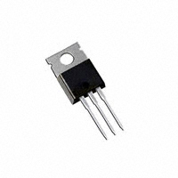


 工商网监
湘ICP备2023018690号
工商网监
湘ICP备2023018690号