PD- 9.1694A
PRELIMINARY
l l l l
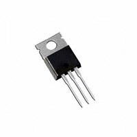
IRL3102
HEXFET® Power MOSFET
D
Advanced Process Technology Optimized for 4.5V-7.0V Gate Drive Ideal for CPU Core DC-DC Converters Fast Switching
G
VDSS = 20V RDS(on) = 0.013Ω
S
Description
These HEXFET Power MOSFETs were designed specifically to meet the demands of CPU core DC-DC converters in the PC environment. Advanced processing techniques combined with an optimized gate oxide design results in a die sized specifically to offer maximum efficiency at minimum cost. The TO-220 package is universally preferred for all commercial-industrial applications at power dissipation levels to approximately 50 watts. The low thermal resistance and low package cost of the TO220 contribute to its wide acceptance throughout the industry.
TO-220AB
ID = 61A
Absolute Maximum Ratings
Parameter
ID @ TC = 25°C ID @ TC = 100°C IDM PD @TC = 25°C VGS VGSM EAS IAR EAR dv/dt TJ TSTG Continuous Drain Current, VGS @ 4.5V Continuous Drain Current, VGS @ 4.5V Pulsed Drain Current Power Dissipation Linear Derating Factor Gate-to-Source Voltage Gate-to-Source Voltage (Start Up Transient, tp = 100µs) Single Pulse Avalanche Energy Avalanche Current Repetitive Avalanche Energy Peak Diode Recovery dv/dt Operating Junction and Storage Temperature Range Soldering Temperature, for 10 seconds Mounting torque, 6-32 or M3 srew
Max.
61 39 240 89 0.71 ± 10 14 220 35 8.9 5.0 -55 to + 150 300 (1.6mm from case ) 10 lbf•in (1.1N•m)
Units
A W W/°C V V mJ A mJ V/ns °C
Thermal Resistance
Parameter
RθJC RθCS RθJA Junction-to-Case Case-to-Sink, Flat, Greased Surface Junction-to-Ambient
Typ.
––– 0.50 –––
Max.
1.4 ––– 62
Units
°C/W
11/18/97
�IRL3102
Electrical Characteristics @ TJ = 25°C (unless otherwise specified)
Parameter Drain-to-Source Breakdown Voltage ∆V(BR)DSS/∆TJ Breakdown Voltage Temp. Coefficient V(BR)DSS RDS(on) VGS(th) gfs IDSS IGSS Qg Qgs Qgd td(on) tr td(off) tf LD LS Ciss Coss Crss Static Drain-to-Source On-Resistance Gate Threshold Voltage Forward Transconductance Drain-to-Source Leakage Current Gate-to-Source Forward Leakage Gate-to-Source Reverse Leakage Total Gate Charge Gate-to-Source Charge Gate-to-Drain ("Miller") Charge Turn-On Delay Time Rise Time Turn-Off Delay Time Fall Time Internal Drain Inductance Internal Source Inductance Input Capacitance Output Capacitance Reverse Transfer Capacitance Min. 20 ––– ––– ––– 0.70 36 ––– ––– ––– ––– ––– ––– ––– ––– ––– ––– ––– ––– ––– ––– ––– ––– Typ. ––– 0.016 ––– ––– ––– ––– ––– ––– ––– ––– ––– ––– ––– 10 130 80 110 Max. Units Conditions ––– V VGS = 0V, ID = 250µA ––– V/°C Reference to 25°C, ID = 1mA 0.015 VGS = 4.5V, ID = 37A Ω 0.013 VGS = 7.0V, ID = 37A ––– V VDS = VGS, ID = 250µA ––– S VDS = 16V, ID = 35A 25 VDS = 20V, VGS = 0V µA 250 VDS = 10V, VGS = 0V, TJ = 150°C 100 VGS = 10V nA -100 VGS = -10V 58 ID = 35A 14 nC VDS = 16V 21 VGS = 4.5V, See Fig. 6 ––– VDD = 10V ––– ID = 35A ns ––– RG = 9.0Ω, VGS = 4.5V ––– RD = 0.28Ω, Between lead, 4.5 ––– 6mm (0.25in.) nH G from package 7.5 ––– and center of die contact 2500 ––– VGS = 0V 1000 ––– pF VDS = 15V 360 ––– ƒ = 1.0MHz, See Fig. 5
D
S
Source-Drain Ratings and Characteristics
IS
I SM
V SD t rr Qrr ton
Parameter Continuous Source Current (Body Diode) Pulsed Source Current (Body Diode) Diode Forward Voltage Reverse Recovery Time Reverse Recovery Charge Forward Turn-On Time
Min. Typ. Max. Units
Conditions D MOSFET symbol 61 ––– ––– showing the A G integral reverse ––– ––– 240 S p-n junction diode. ––– ––– 1.3 V TJ = 25°C, IS = 37A, VGS = 0V ––– 59 88 ns TJ = 25°C, IF = 35A ––– 110 160 nC di/dt = 100A/µs Intrinsic turn-on time is negligible (turn-on is dominated by LS+LD)
Notes:
Repetitive rating; pulse width limited by
max. junction temperature.
ISD ≤ 35A, di/dt ≤ 100A/µs, VDD ≤ V(BR)DSS,
TJ ≤ 150°C
Starting TJ = 25°C, L = 0.36mH
RG = 25Ω, IAS = 35A.
Pulse width ≤ 300µs; duty cycle ≤ 2%.
�IRL3102
1000
VGS VGS 15V 10V 12V 8.0V 10V 6.0V 8.0V 4.0V 6.0V 3.0V 4.0V 3.0V BOTTOM 2.5V BOTTOM 2.5V TOP TOP
1000
I D , Drain-to-Source Current (A)
100
I D , Drain-to-Source Current (A)
VGS VGS 15V 10V 12V 8.0V 10V 6.0V 8.0V 4.0V 6.0V 4.0V 3.0V 3.0V BOTTOM 2.5V BOTTOM 2.5V TOP TOP
100
2.5V
20µs PULSE WIDTH TJ = 25 °C
1 10 100
2.5V
20µs PULSE WIDTH TJ = 150 °C
1 10 100
10 0.1
10 0.1
VDS , Drain-to-Source Voltage (V)
VDS , Drain-to-Source Voltage (V)
Fig 1. Typical Output Characteristics
Fig 2. Typical Output Characteristics
1000
2.0
TJ = 25 ° C
R DS(on) , Drain-to-Source On Resistance (Normalized)
ID = 61A
I D , Drain-to-Source Current (A)
1.5
100
TJ = 150 ° C
1.0
10
0.5
1 2 3 4
V DS = 15V 20µs PULSE WIDTH 5 6 7
0.0 -60 -40 -20
VGS = 4.5V
0 20 40 60 80 100 120 140 160
VGS , Gate-to-Source Voltage (V)
TJ , Junction Temperature( °C)
Fig 3. Typical Transfer Characteristics
Fig 4. Normalized On-Resistance Vs. Temperature
�IRL3102
4200
3600
VGS , Gate-to-Source Voltage (V)
VGS = Ciss = Crss = Coss =
0V, f = 1MHz Cgs + Cgd , Cds SHORTED Cgd Cds + Cgd
15
ID = 35A VDS = 16V
12
C, Capacitance (pF)
3000
Ciss
2400
9
1800
Coss
1200
6
600
Crss
3
0 1 10 100
0 0 20 40 60 80 100
VDS , Drain-to-Source Voltage (V)
QG , Total Gate Charge (nC)
Fig 5. Typical Capacitance Vs. Drain-to-Source Voltage
Fig 6. Typical Gate Charge Vs. Gate-to-Source Voltage
1000
1000
ISD , Reverse Drain Current (A)
OPERATION IN THIS AREA LIMITED BY RDS(on)
100
I D , Drain Current (A)
100
TJ = 150 ° C
100us
1ms 10
TJ = 25 ° C
10
10ms
1 0.2
V GS = 0 V
0.8 1.4 2.0 2.6 1 1
TC = 25 ° C TJ = 150 ° C Single Pulse
10 100
VSD ,Source-to-Drain Voltage (V)
VDS , Drain-to-Source Voltage (V)
Fig 7. Typical Source-Drain Diode Forward Voltage
Fig 8. Maximum Safe Operating Area
�IRL3102
70
500
EAS , Single Pulse Avalanche Energy (mJ)
TOP
400
60
BOTTOM
ID 16A 22A 35A
I D , Drain Current (A)
50
40
300
30
200
20
100
10
0 25 50 75 100 125 150
0 25 50 75 100 125 150
TC , Case Temperature ( ° C)
Starting T , Junction Temperature( °C) J
Fig 9. Maximum Drain Current Vs. Case Temperature
Fig 10. Maximum Avalanche Energy Vs. Drain Current
10
Thermal Response (Z thJC )
1
D = 0.50 0.20 0.10 P DM t1 SINGLE PULSE (THERMAL RESPONSE) Notes: 1. Duty factor D = t 1 / t 2 2. Peak T J = P DM x Z thJC + TC 0.0001 0.001 0.01 0.1 1 t2
0.1
0.05 0.02 0.01
0.01 0.00001
t1 , Rectangular Pulse Duration (sec)
Fig 11. Maximum Effective Transient Thermal Impedance, Junction-to-Case
�IRL3102
R DS (on) , Drain-to-Source On Resistance( Ω )
RDS(on), Drain-to-Source On Resistance ( Ω )
0.015
0.020
0.014
0.018
VGS = 4.5V
0.013
0.016
0.014
0.012
0.012
ID = 6 1A
0.011
VGS = 7.0V
0.010 0 20 40 60 80
0.010
0.008 0 2 4 6 8 10
A
I D , Drain Current (A)
V G S , G ate-to-Source V olta g e (V )
Fig 12. On-Resistance Vs. Drain Current
Fig 13. On-Resistance Vs. Gate Voltage
�IRL3102
Package Outline
TO-220AB Outline Dimensions are shown in millimeters (inches)
2.87 (.11 3) 2.62 (.10 3) 10.54 (.415) 10.29 (.405) 3.7 8 (.149 ) 3.5 4 (.139 ) -A 6.47 (.255) 6.10 (.240) -B4.69 (.185 ) 4.20 (.165 ) 1.32 (.052) 1.22 (.048)
4 15.24 (.60 0) 14.84 (.58 4)
1.15 (.04 5) M IN 1 2 3
LE A D A S S IG N M E N T S 1 - G ATE 2 - D R A IN 3 - SOURCE 4 - D R A IN
14.09 (.55 5) 13.47 (.53 0)
4.06 (.160) 3.55 (.140)
3X 3X 1 .40 (.0 55) 1 .15 (.0 45)
0.93 (.037) 0.69 (.027) M BAM
3X
0.55 (.022) 0.46 (.018)
0.36 (.014)
2.54 (.100) 2X NO TES: 1 D IM E N S IO N IN G & T O LE R A N C IN G P E R A N S I Y 14.5M , 1 982. 2 C O N TR O LLIN G D IM E N S IO N : IN C H
2.92 (.115) 2.64 (.104)
3 O U T LIN E C O N F O R M S TO JE D E C O U T LIN E T O -2 20A B . 4 H E A T S IN K & LE A D M E A S U R E M E N T S D O NO T IN C LU D E B U R R S .
Part Marking Information
TO-220AB
EXAMP : TH IS N 1 0 1 0 E X A M P L E :L ETH IS IS A N AIR F IR F 1 0 1 0 W A ASSEMB W ITH ITHS S E M B L Y L Y L C CO B M L O T O TO D E D9E 19 B 1 M
A A
IN TE R N A N A N IN TE R N A T IO T IOL A L RECT R R E C TIF IEIF IE R IR F IR F 1 0 1 0 1010 L LOGO GO 9 2 49 2 4 6 6 9 B 9 B1 M 1 M ASSEMB ASSEMBLY LY L C CO LOT OT ODE DE
PA N NUMB P A R T R TU M B E R E R
DA C CO D A TE TEO D E D E (Y Y(Y Y W W ) WW) Y Y Y Y Y= A R A R = E YE W W W E WK E K WW = = E E
WORLD HEADQUARTERS: 233 Kansas St., El Segundo, California 90245, Tel: (310) 322 3331 EUROPEAN HEADQUARTERS: Hurst Green, Oxted, Surrey RH8 9BB, UK Tel: ++ 44 1883 732020 IR CANADA: 7321 Victoria Park Ave., Suite 201, Markham, Ontario L3R 2Z8, Tel: (905) 475 1897 IR GERMANY: Saalburgstrasse 157, 61350 Bad Homburg Tel: ++ 49 6172 96590 IR ITALY: Via Liguria 49, 10071 Borgaro, Torino Tel: ++ 39 11 451 0111 IR FAR EAST: K&H Bldg., 2F, 30-4 Nishi-Ikebukuro 3-Chome, Toshima-Ku, Tokyo Japan 171 Tel: 81 3 3983 0086 IR SOUTHEAST ASIA: 315 Outram Road, #10-02 Tan Boon Liat Building, Singapore 0316 Tel: 65 221 8371 http://www.irf.com/ Data and specifications subject to change without notice. 11/97
�