IRL3103D2PbF
l l l l l l
PD-95435
Copackaged HEXFET® Power MOSFET and Schottky Diode Generation 5 Technology Logic Level Gate Drive Minimize Circuit Inductance Ideal For Synchronous Regulator Application Lead-Free
FETKYTM MOSFET & SCHOTTKY RECTIFIER
D
VDSS = 30V RDS(on) = 0.014Ω
G
ID = 54A
S
Description
The FETKY family of copackaged HEXFET power MOSFETs and Schottky Diodes offer the designer an innovative board space saving solution for switching regulator applications. A low on resistance Gen 5 MOSFET with a low forward voltage drop Schottky diode and minimized component interconnect inductance and resistance result in maximized converter efficiencies. The TO-220 package is universally preferred for all commercial-industrial applications at power dissipation levels to approximately 50 watts. The low thermal resistance and low package cost of the TO-220 contribute to its wide acceptance throughout the industry.
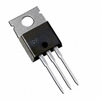
TO-220AB
Absolute Maximum Ratings
Parameter
ID @ TC = 25°C ID @ TC = 100°C IDM PD @TA = 25°C PD @TC = 25°C VGS TJ TSTG Continuous Drain Current, VGS @ 10V Continuous Drain Current, VGS @ 10V Pulsed Drain Current Power Dissipation Power Dissipation Linear Derating Factor Gate-to-Source Voltage Operating Junction and Storage Temperature Range Soldering Temperature, for 10 seconds Mounting torque, 6-32 or M3 srew
Max.
54 34 220 2.0 70 0.56 ± 16 -55 to + 150 300 (1.6mm from case ) 10 lbfin (1.1Nm)
Units
A W W W/°C V
°C
Thermal Resistance
Parameter
RθJC RθJA Junction-to-Case Junction-to-Ambient
Typ.
Max.
1.8 62
Units
°C/W
06/22/04
�IRL3103D2PbF
MOSFET Electrical Characteristics @ TJ = 25°C (unless otherwise specified)
V(BR)DSS
∆V(BR)DSS/∆TJ
Parameter Drain-to-Source Breakdown Voltage Breakdown Voltage Temp. Coefficient Static Drain-to-Source On-Resistance Gate Threshold Voltage Forward Transconductance Drain-to-Source Leakage Current Gate-to-Source Forward Leakage Gate-to-Source Reverse Leakage Total Gate Charge Gate-to-Source Charge Gate-to-Drain ("Miller") Charge Turn-On Delay Time Rise Time Turn-Off Delay Time Fall Time Internal Drain Inductance Internal Source Inductance Input Capacitance Output Capacitance Reverse Transfer Capacitance Input Capacitance
RDS(on) VGS(th) gfs IDSS IGSS Qg Qgs Qgd td(on) tr td(off) tf LD LS Ciss Coss Crss Ciss
Min. 30 1.0 23
Typ. 0.037 9.0 210 20 54 4.5 7.5 2300 1100 310 3500
Max. Units Conditions V V GS = 0V, ID = 250µA V/°C Reference to 25°C, ID = 1mA 0.014 V GS = 10V, ID = 32A Ω 0.019 V GS = 4.5V, ID = 27A V V DS = V GS, ID = 250µA S V DS = 25V, ID = 34A 0.25 V DS = 30V, VGS = 0V mA 35 V DS = 24V, VGS = 0V, TJ = 125°C 100 V GS = 16V nA -100 V GS = -16V 44 I D = 32A 14 nC V DS = 24V 24 V GS = 4.5V, See Fig. 6 V DD = 15V ID = 34A ns R G = 3.4Ω, V GS =4.5V R D = 0.43 Ω, Between lead, 6mm (0.25in.) nH G from package and center of die contact V GS = 0V V DS = 25V pF = 1.0MHz, See Fig. 5 V GS = 0V, VDS = 0V
D
S
Body Diode & Schottky Diode Ratings and Characteristics
Parameter IF (AV)
ISM
Min. Typ. Max. Units
( Schottky) Pulsed Source Current (Body Diode) Diode Forward Voltage Diode Forward Voltage Reverse Recovery Time Reverse Recovery Charge Forward Turn-On Time
VSD1 VSD2 trr Qrr ton
Conditions MOSFET symbol 5.0 showing the A integral reverse 220 p-n junction and Schottky diode. 1.3 V TJ = 25°C, IS = 32A, VGS = 0V 0.6 V TJ = 25°C, IS = 3.0A, VGS = 0V 51 77 ns TJ = 25°C, IF = 32A 47 71 nC di/dt = 100A/µs Intrinsic turn-on time is negligible (turn-on is dominated by LS+LD)
D G
S
Notes: Repetitive rating; pulse width limited by max. junction temperature. ( See fig. 10 )
Pulse width ≤ 300µs; duty cycle ≤ 2%.
Uses IRL3103 data and test conditions
�IRL3103D2PbF
1000
VGS 15V 12V 10V 8.0V 6.0V 4.0V 3.0V BOTTOM 2.5V TOP
1000
100
ID , Drain-to-Source Current (A)
ID , Drain-to-Source Current (A)
VGS 15V 12V 10V 8.0V 6.0V 4.0V 3.0V BOTTOM 2.5V TOP
100
10
10
2.5V
2.5V
1 0.1
20µs PULSE WIDTH T J = 25°C
1 10
A
100
1 0.1
20µs PULSE WIDTH TJ = 150°C
1 10
A
100
VDS , Drain-to-Source Voltage (V)
VDS , Drain-to-Source Voltage (V)
Fig 1. Typical Output Characteristics
Fig 2. Typical Output Characteristics
30
30
IS, Source-to-Drain Current ( A )
20
IS, Source-to-Drain Current ( A )
VGS 10V 8.0V 6.0V 4.0V 2.0V BOTTOM 0.0V TOP
20
0.0V
10
VGS 10V 8.0V 6.0V 4.0V 2.0V BOTTOM 0.0V TOP
0.0V
10
0 0.0
20µs PULSE WIDTH TC = 25°C
0.2 0.4 0.6 0.8 1.0
A
0 0.0
20µs PULSE WIDTH TC = 150°C
0.2 0.4 0.6 0.8
A
VDS, Drain-to-Source Voltage (V)
VDS, Drain-to-Source Voltage (V)
Fig 3. Typical Reverse Output Characteristics
Fig 4. Typical Reverse Output Characteristics
�IRL3103D2PbF
5000
VGS , Gate-to-Source Voltage (V)
C, Capacitance ( pF )
4000
V GS = 0V, f = 1MHz C iss = C gs + C gd , C ds SHORTED C rss = C gd C oss = C ds + C gd
15
ID = 32A VDS = 24V VDS = 15V
12
3000
9
Ciss Coss
2000
6
1000
3
Crss
0 1 10 100
A
0 0 20 40 60 80
VDS , Drain-to-Source Voltage (V)
QG , Total Gate Charge (nC)
Fig 5. Typical Capacitance Vs. Drain-to-Source Voltage
Fig 6. Typical Gate Charge Vs. Gate-to-Source Voltage
60
1000
I D , Drain-to-Source Current (A)
50
ID , Drain Current (A)
TJ = 25°C
100
40
TJ = 150°C
30
20
10
10
0 25 50 75 100 125 150
1 2.0 3.0 4.0 5.0
VDS = 15V 20µs PULSE WIDTH
6.0 7.0 8.0 9.0
A
TC , Case Temperature ( ° C)
VGS , Gate-to-Source Voltage (V)
Fig 7. Maximum Drain Current Vs. Case Temperature
Fig 8. Typical Transfer Characteristics
�IRL3103D2PbF
2.0
RDS(on) , Drain-to-Source On Resistance (Normalized)
ID = 54A
1.5
1.0
0.5
0.0 -60 -40 -20
VGS = 10V
0 20 40 60 80 100 120 140 160
TJ , Junction Temperature ( °C)
Fig 9. Normalized On-Resistance Vs. Temperature
10
Thermal Response (ZthJC )
1
D = 0.50
0.20 0.10
0.1
P DM
0.05 0.02 0.01 SINGLE PULSE (THERMAL RESPONSE)
Notes: 1. Duty factor D = t /t
t
1 t2
1
2
0.01 0.00001
2. Peak TJ = P DM x Z thJC + T C
A
1
0.0001
0.001
0.01
0.1
t 1 , Rectangular Pulse Duration (sec)
Fig 10. Maximum Effective Transient Thermal Impedance, Junction-to-Case
�IRL3103D2PbF
TO-220AB Package Outline
Dimensions are shown in millimeters (inches)
10.54 (.415) 10.29 (.405) 3.78 (.149) 3.54 (.139) -A6.47 (.255) 6.10 (.240) -B4.69 (.185) 4.20 (.165) 1.32 (.052) 1.22 (.048)
2.87 (.113) 2.62 (.103)
4 15.24 (.600) 14.84 (.584)
LEAD ASSIGNMENTS
1.15 (.045) MIN 1 2 3 LEAD ASSIGNMENTS IGBTs, CoPACK 1 - GATE 2 1- GATE- DRAIN 1- GATE 32- DRAINSOURCE 2- COLLECTOR 3- SOURCE 3- EMITTER 4 - DRAIN
HEXFET
14.09 (.555) 13.47 (.530)
4- DRAIN
4.06 (.160) 3.55 (.140)
4- COLLECTOR
3X 3X 1.40 (.055) 1.15 (.045)
0.93 (.037) 0.69 (.027) M BAM
3X
0.55 (.022) 0.46 (.018)
0.36 (.014)
2.54 (.100) 2X NOTES: 1 DIMENSIONING & TOLERANCING PER ANSI Y14.5M, 1982. 2 CONTROLLING DIMENSION : INCH
2.92 (.115) 2.64 (.104)
3 OUTLINE CONFORMS TO JEDEC OUTLINE TO-220AB. 4 HEATSINK & LEAD MEASUREMENTS DO NOT INCLUDE BURRS.
TO-220AB Part Marking Information
E X AMP L E : T H IS IS AN IR F 1010 L OT CODE 1789 AS S E MB L E D ON WW 19, 1997 IN T H E AS S E MB L Y L INE "C" INT E R NAT ION AL R E CT IF IE R L OGO AS S E MB L Y L OT CODE P AR T NU MB E R
Note: "P" in assembly line position indicates "Lead-Free"
DAT E CODE YE AR 7 = 1997 WE E K 19 L INE C
Data and specifications subject to change without notice.
IR WORLD HEADQUARTERS: 233 Kansas St., El Segundo, California 90245, USA Tel: (310) 252-7105 TAC Fax: (310) 252-7903 Visit us at www.irf.com for sales contact information. 06/04
�Note: For the most current drawings please refer to the IR website at: http://www.irf.com/package/
�