Data Sheet No. PD60347
IRS26310DJPbF
HIGH VOLTAGE 3 PHASE GATE DRIVER IC WITH DC BUS OVER –VOLTAGE PROTECTION Features
• • • • • • • • • • • • • • • • • • • Drives up to six IGBT/MOSFET power devices Gate drive supplies up to 20 V per channel Integrated bootstrap functionality DC bus sensing with Over Voltage protection Over-current protection Over-temperature shutdown input Advanced input filter Integrated deadtime protection Shoot-through (cross-conduction) protection Under voltage lockout for VCC & VBS Enable/disable input and fault reporting Adjustable fault clear timing Separate logic and power grounds 3.3 V input logic compatible Tolerant to negative transient voltage Designed for use with bootstrap power supplies Matched propagation delays for all channels -40 °C to 125 °C operating range RoHS compliant
Product Summary
Topology VOFFSET VOUT Io+ & I o- (typical) tON & tOFF (typical) Deadtime (typical) 3 Phase ≤ 600 V 12 V – 20 V 200 mA & 350 mA 530 ns & 530 ns 290 ns
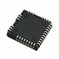
Package Options
44-Lead PLCC (without 12 leads)
Typical Applications
• • • Permanent magnet motor drives for appliances Industrial drives Micro inverter drives
Typical Connection Diagram
Rev.1.0
�IRS26310DJPbF
Table of Contents
Description Simplified Block Diagram Typical Application Diagram Qualification Information Absolute Maximum Ratings Recommended Operating Conditions Static Electrical Characteristics Dynamic Electrical Characteristics Functional Block Diagram Input/Output Pin Equivalent Circuit Diagram Lead Definitions Lead Assignments Application Information and Additional Details Parameter Temperature Trends Package Details Tape and Reel Details Part Marking Information Ordering Information
Page
3 3 4 5 6 7 8 10 11 12 13 14 15 34 38 39 40 41
www.irf.com
© 2007 International Rectifier
2
�IRS26310DJPbF
Description
The IRS26310DJPBF is a high voltage, high speed power MOSFET and IGBT driver with three independent high and low side referenced output channels for 3-phase applications. This IC is designed to be used with low-cost bootstrap power supplies; the bootstrap diode functionality has been integrated into this device to reduce the component count and the PCB size. Proprietary HVIC technology enables ruggedized monolithic construction. Logic inputs are compatible with CMOS or LSTTL outputs, down to 3.3 V logic. A current trip function which terminates all six outputs can be derived from an external current sense resistor. An enable function is available to terminate all six outputs simultaneously. An open-drain FAULT signal is provided to indicate that an overcurrent or a VCC undervoltage shutdown has occurred. Overcurrent fault conditions are cleared automatically after a delay programmed externally via an RC network connected to the RCIN input. The output drivers feature a high pulse current buffer stage designed for minimum driver cross-conduction. Propagation delays are matched to simplify use in high frequency applications. The floating channel can be used to drive N-channel power MOSFETs or IGBTs in the high side configuration which operates up to 600 V. A DCbus sensing is provided using an external divider. Over Voltage DCbus protection is activate when DCbus exceed an externally adjustable threshold, activating zero-vector braking mode (all Low side output turn-on, all High side output-turn-off).
Simplified Block Diagram
www.irf.com
© 2007 International Rectifier
3
�IRS26310DJPbF
Typical Application Diagram
www.irf.com
© 2007 International Rectifier
4
�IRS26310DJPbF
Qualification Information†
Qualification Level Industrial†† Comments: This family of ICs has passed JEDEC’s Industrial qualification. IR’s Consumer qualification level is granted by extension of the higher Industrial level. PLCC44 Machine Model ESD Human Body Model Charged Device Model IC Latch-Up Test RoHS Compliant † †† MSL3††† , 245°C (per IPC/JEDEC J-STD-020)
Moisture Sensitivity Level
Class B (per JEDEC standard JESD22-A114) Class 2 (per EIA/JEDEC standard EIA/JESD22-A115) Class IV (per JEDEC standard JESD22-C101) Class I, Level A (per JESD78) Yes
Qualification standards can be found at International Rectifier’s web site http://www.irf.com/ Higher qualification ratings may be available should the user have such requirements. Please contact your International Rectifier sales representative for further information. ††† Higher MSL ratings may be available for the specific package types listed here. Please contact your International Rectifier sales representative for further information.
www.irf.com
© 2007 International Rectifier
5
�IRS26310DJPbF
Absolute Maximum Ratings
Absolute maximum ratings indicate sustained limits beyond which damage to the device may occur. All voltage parameters are absolute voltages referenced to VSS unless otherwise stated in the table. The thermal resistance and power dissipation ratings are measured under board mounted and still air conditions. Voltage clamps are included between VCC & COM (25 V), VCC & VSS (20 V), and VB & VS (20 V). Symbol VS VTST VB VHO VCC VSS VLO1,2,3 VIN VFLT VDCBusSense dV/dt PD RthJA TJ TS TL † TST Voltage High side floating supply voltage High side floating output voltage Low side and logic fixed supply voltage Logic ground Low side output voltage Input voltage LIN, HIN, ITRIP, EN, RCIN FAULT output voltage Input sensing for DCBUS voltage Allowable offset voltage slew rate Package power dissipation @ TA ≤ +25°C Thermal resistance, junction to ambient Junction temperature Storage temperature Lead temperature (soldering, 10 seconds) Definition High side offset voltage Min. VB - 20† -0.3 -0.3 VS - 0.3 -0.3 VCC - 20 -0.3 VSS -0.3 VSS -0.3 VSS -0.3 — — — — -55 — Max. VB + 0.3 20 620 VB + 0.3 20 VCC + 0.3 VCC + 0.3 VCC + 0.3 VCC + 0.3 VCC + 0.3 50 2 63 150 150 300 Units
V
V/ns W °C/W °C
All supplies are fully tested at 25 V. An internal 20 V clamp exists for each supply.
www.irf.com
© 2007 International Rectifier
6
�IRS26310DJPbF
Recommended Operating Conditions
For proper operation, the device should be used within the recommended conditions. All voltage parameters are absolute voltages referenced to VSS unless otherwise stated in the table. The offset rating is tested with supplies of (VCC-COM) = (VB-VS) = 15 V. Symbol VB VS VS(t) VTST VCC VHO VLO VSS VFLT VRCIN VITRIP VIN VDCBusSense TA † Definition High side floating supply voltage † High side floating supply voltage †† Transient high-side floating supply voltage TST Voltage Low side supply voltage High side output voltage Low side output voltage Logic ground FAULT output voltage RCIN input voltage ITRIP input voltage Logic input voltage LIN, HIN, EN Input sensing for DCbus voltage††† Ambient temperature Min. VS +12 COM-8 -50 12 12 VS 0 -5 VSS VSS VSS VSS VSS -40 Max. VS + 20 600 600 20 20 VB VCC 5 VCC VCC VSS + 5 VSS + 5 VCC 125 Units
V
°C
Logic operation for VS of –8 V to 600 V. Logic state held for VS of –8 V to –VBS. Please refer to Design Tip DT97-3 for more details. †† Operational for transient negative VS of VSS - 50 V with a 50 ns pulse width. Guaranteed by design. Refer to the Application Information section of this datasheet for more details. ††† DCBusSense pin is internally clamped with a 10.4 V zener diode.
www.irf.com
© 2007 International Rectifier
7
�IRS26310DJPbF
(VCC-COM) = (VB-VS) = 15 V. TA = 25 oC unless otherwise specified. The VIN ,VTH and IIN parameters are referenced to VSS and are applicable to all six channels. The VO and IO parameters are referenced to respective VS and COM and are applicable to the respective output leads HO or LO. The VCCUV parameters are referenced to VSS. The VBSUV parameters are referenced to VS. Symbol VIH VIL VIN,TH+ VIN,THVEN,TH+ VEN,THVIT,TH+ VIT,HYS VRCIN, TH+ VRCIN, HYS VOH VOL VCCUV+ VCCUVVCCUVHYS VBSUV+ VBSUVVBSUVHY VDCBUSSTH+ Definition Logic “1” input Logic “0” input Input positive going threshold Input negative going threshold Enable positive going threshold Enable negative going threshold ITRIP positive going threshold ITRIP hysteresis RCIN positive going threshold RCIN hysteresis High level output voltage, VBIAS – VO Low level output voltage, VO VCC supply undervoltage positive going threshold VCC supply undervoltage negative going threshold VCC supply undervoltage hysteresis VBS supply undervoltage positive going threshold VBS supply undervoltage negative going threshold VBS supply undervoltage hysteresis Min. 2.5 — — — — 0.8 0.37 0.05 — — — — 10.4 10.2 0.17 10.4 10.2 0.17 Typ. — — 1.9 1 — — 0.46 0.07 8 3 1.12 0.4 11.1 10.9 0.2 11.1 10.9 0.2 Max. — 0.8 — — 2.5 — 0.55 — — — 1.74 0.6 11.6 11.4 — 11.6 11.4 — 4.54 4.35 — 50 120 4 150 — 40 — 1 — 1 — Note 1 V Units Test Conditions
Static Electrical Characteristics
IO = 20 mA
Over voltage DCBusSense positive going 3.86 4.20 threshold Over voltage DCBusSense negative going 3.70 4.03 VDCBUSSTHthreshold VDCBUSSHYS Over voltage DCBusSense hysteresis 0.14 0.17 ILK Offset supply leakage current — 3 IQBS Quiescent VBS supply current — 50 IQCC Quiescent VCC supply current — 3 IIN+ Input bias current (Lo or Ho= High) — 100 IINInput bias current (Lo or Ho = Low) -1 0 IITRIP+ “High” ITRIP input bias current — 5 IITRIP“Low” ITRIP input bias current -1 0 IFLT/EN+ “High” FLT/ENABLE input bias current — 0 IFLT/EN“Low” FLT/ENABLE input bias current -1 0 IDCBUSSENSE+ “High” DCBusSense input bias current — 0 IDCBUSSENSE“Low” DCBusSense input bias current -1 0 Note 1: Guaranteed by design over a temperature range of 0ºC to 110ºC
www.irf.com
VB =VS = 600 V mA All inputs @ logic 0 value VIN = 3.3 V VIN = 0 V VITRIP = 5 V VITRIP = 0 V VFLT/EN = 3.3 V VFLT/EN = 0 V VDCBSENSE = 5 V VDCBSENSE = 0 V
uA
© 2007 International Rectifier
8
�IRS26310DJPbF
Static Electrical Characteristics (continued)
(VCC-COM) = (VB-VS) = 15 V. TA = 25 oC unless otherwise specified. The VIN ,VTH and IIN parameters are referenced to VSS and are applicable to all six channels. The VO and IO parameters are referenced to respective VS and COM and are applicable to the respective output leads HO or LO. The VCCUV parameters are referenced to VSS. The VBSUV parameters are referenced to VS. Symbol IRCIN+ IRCINIo+ IoRon_RCIN Ron_FAULTEN RBS Definition “High” RCIN input bias current “Low” RCIN input bias current Output high short circuit pulsed current Output low short circuit pulsed current RCIN low on resistance FAULT low on resistance Internal bootstrap diode Ron Min. — -1 120 250 — — — Typ. 0 0 200 350 50 50 200 Max. 1 — — mA — 100 100 400 Ω Units uA Test Conditions VRCIN = 15 V VRCIN = 0 V Vo = 0 V, PW ≤ 10 µs Vo = 15 V, PW ≤ 10 µs I = 1.5 mA
www.irf.com
© 2007 International Rectifier
9
�IRS26310DJPbF
Dynamic Electrical Characteristics
Symbol ton toff tr tf tITRIP tITRIP_blk tFLT tENOUT tSDOUT tZV_DCBS_LOon tZV_DCBS_HOoff tZV_DCBS_HOon tZV_DCBS_LOoff tZV_DCBS_flt_LO tZV_DCBS_flt_HO tFILIN tFILTEREN DT MT MDT PM tFLTCLR Definition Turn-on propagation delay Turn-off propagation delay Turn-on rise time Turn-off fall time ITRIP to output shutdown propagation delay ITRIP blanking time ITRIP to FAULT propagation delay ENABLE high to output propagation delay ENABLE low to output shutdown propagation delay DCBusSense entering Over voltage to LO turn on DCBusSense entering Over voltage to HO turn off DCBusSense exiting Over voltage to HO turn on DCBusSense exiting Over voltage to LO turn off DCBusSense input filter time on LO DCBUSSENSE input filter time on HO † Input filter time (HIN, LIN) Enable input filter time Deadtime Ton, Toff matching time (on all six channels) DT matching (HIN->LO & LO>HIN on all channels) †† Pulse width distortion FAULT clear time RCIN: R = 2 meg, C = 1nF VCC= VB = 15 V, VS = VSS = COM, TA = 25 oC, and CL = 1000 pF unless otherwise specified. Min. 400 400 — — 500 — 400 350 350 310 310 270 300 140 140 200 100 190 — — — 1.3 Typ. 530 530 125 50 750 500 600 460 460 460 460 380 450 250 250 350 200 290 — — — 1.65 Max. 750 750 190 75 1200 750 950 650 650 730 730 590 VDCBSENSE = 0V & 5V 720 420 420 510 — 420 50 60 75 2 ms PW input =10µs VIN = 0V or 5V VITRIP = 0V ns VIN = 0V & 5V ns Units Test Conditions VIN = 0V & 5V
VITRIP = 5V VIN = 0V & 5V VITRIP = 5V VIN = 0V & 5V VEN = 0V & 3.3V
VIN = 0V & 5V External dead time 0s
† ††
The minimum width of the input pulse is recommended to exceed 500 ns to ensure the filtering time of the input filter is exceeded. PM is defined as PWIN - PWOUT.
www.irf.com
© 2008 International Rectifier
10
�IRS26310DJPbF
Functional Block Diagram: IRS26310DJ
www.irf.com
© 2008 International Rectifier
11
�IRS26310DJPbF
Input/Output Pin Equivalent Circuit Diagrams: IRS26310D
www.irf.com
© 2008 International Rectifier
12
�IRS26310DJPbF
Lead Definitions: IRS26310DJ
Symbol VCC VSS TST VB1 VB2 VB3 VS1 VS2 VS3 HIN1 HIN2 HIN3 LIN1 LIN2 LIN3 HO1 HO2 HO3 LO1 LO2 LO3 COM FAULT/N EN Description Low-side supply voltage Logic ground TST to be shorted to VCC High-side gate drive floating supply (phase 1) High-side gate drive floating supply (phase 2) High-side gate drive floating supply (phase 3) High voltage floating supply return (phase 1) High voltage floating supply return (phase 2) High voltage floating supply return (phase 3) Logic inputs for high-side gate driver outputs (phase 1) Logic inputs for high-side gate driver outputs (phase 2) Logic inputs for high-side gate driver outputs (phase 3 Logic inputs for low-side gate driver outputs (phase 1) Logic inputs for low-side gate driver outputs (phase 2) Logic inputs for low-side gate driver outputs (phase 3) High-side driver outputs (phase 1) High-side driver outputs (phase 2) High-side driver outputs (phase 3) Low-side driver outputs (phase 1) Low-side driver outputs (phase 2) Low-side driver outputs (phase 3) Low-side gate drive return Indicates over-current, over-temperature (ITRIP), or low-side undervoltage lockout has occurred. This pin has negative logic and an open-drain output. The use of over-current and overtemperature protection requires the use of external components. Logic input to shutdown functionality. Logic functions when EN is high (i.e., positive logic). No effect on FAULT and not latched. Analog input for over-current shutdown. When active, ITRIP shuts down outputs and activates FAULT and RCIN low. When ITRIP becomes inactive, FAULT stays active low for an externally set time tFLTCLR, then automatically becomes inactive (open-drain high impedance). Analog input for DCbus sensing An external RC network input used to define the FAULT CLEAR delay (tFLTCLR) approximately equal to R*C. When RCIN > 8 V, the FAULT pin goes back into an open-drain high-impedance state.
ITRIP DCbusSense RCIN
www.irf.com
© 2008 International Rectifier
13
�IRS26310DJPbF
Lead Assignments
www.irf.com
TST
© 2008 International Rectifier
14
�IRS26310DJPbF
Application Information and Additional Details
Informations regarding the following topics are included as subsections within this section of the datasheet. • • • • • • • • • • • • • • • • • • • • • IGBT/MOSFET Gate Drive Switching and Timing Relationships Deadtime Matched Propagation Delays Input Logic Compatibility Undervoltage Lockout Protection Shoot-Through Protection Enable Input Fault Reporting and Programmable Fault Clear Timer Over-Current Protection Over-Temperature Shutdown Protection DC bus over-voltage Protection Truth Table: Undervoltage lockout, ITRIP, and ENABLE Advanced Input Filter Short-Pulse / Noise Rejection Integrated Bootstrap Functionality Bootstrap Power Supply Design Separate Logic and Power Grounds Tolerant to Negative VS Transients PCB Layout Tips Additional Documentation
IGBT/MOSFET Gate Drive The IRS26310D HVIC is designed to drive up to six MOSFET or IGBT power devices. Figures 1 and 2 illustrate several parameters associated with the gate drive functionality of the HVIC. The output current of the HVIC, used to drive the gate of the power switch, is defined as IO. The voltage that drives the gate of the external power switch is defined as VHO for the high-side power switch and VLO for the low-side power switch; this parameter is sometimes generically called VOUT and in this case does not differentiate between the high-side or low-side output voltage.
VB (or VCC)
VB (or VCC)
IO+
HO (or LO) + HO (or LO)
VHO (or VLO)
VS (or COM) VS (or COM)
IO-
Figure 1: HVIC sourcing current
Figure 2: HVIC sinking current
www.irf.com
© 2008 International Rectifier
15
�IRS26310DJPbF
Switching and Timing Relationships The relationship between the input and output signals of the IRS26310D is illustrated below in Figures 3. From this figure, we can see the definitions of several timing parameters (i.e., PWIN, PWOUT, tON, tOFF, tR, and tF) associated with this device.
Figure 3: Switching time waveforms The following two figures illustrate the timing relationships of some of the functionality of the IRS26310D; this functionality is described in further detail later in this document. During interval A of Figure 4, the HVIC has received the command to turn-on both the high- and low-side switches at the same time; as a result, the shoot-through protection of the HVIC has prevented this condition and both the highand low-side output are held in the off state. Interval B of Figures 4 and 5 shows that the signal on the ITRIP input pin has gone from a low to a high state; as a result, all of the gate drive outputs have been disabled (i.e., see that HOx has returned to the low state; LOx is also held low), the voltage on the RCIN pin has been pulled to 0 V, and a fault is reported by the FAULT output transitioning to the low state. Once the ITRIP input has returned to the low state, the output will remain disabled and the fault condition reported until the voltage on the RCIN pin charges up to VRCIN,TH (see interval C in Figure 6); the charging characteristics are dictated by the RC network attached to the RCIN pin. During intervals D and E of Figure 4, we can see that the enable (EN) pin has been pulled low (as is the case when the driver IC has received a command from the control IC to shutdown); this results in the outputs (HOx and LOx) being held in the low state until the enable pin is pulled high.
www.irf.com
© 2008 International Rectifier
16
�IRS26310DJPbF
Figure 4: Input/output timing diagram
Figure 5: Detailed view of B & C intervals
Deadtime This family of HVICs features integrated deadtime protection circuitry. The deadtime for these ICs is fixed; other ICs within IR’s HVIC portfolio feature programmable deadtime for greater design flexibility. The deadtime feature inserts a time period (a minimum deadtime) in which both the high- and low-side power switches are held off; this is done to ensure that the power switch being turned off has fully turned off before the second power switch is turned on. This minimum deadtime is automatically inserter whenever the external deadtime is shorter than DT; external deadtimes larger than DT are not modified by the gate driver. Figure 6 illustrates the deadtime period and the relationship between the output gate signals. The deadtime circuitry of the IRS26310D is matched with respect to the high- and low-side outputs of a given channel; additionally, the deadtimes of each of the three channels are matched. Figure 6 defines the two deadtime parameters (i.e., DT1 and DT2) of a specific channel; the deadtime matching parameter (MDT) associated with the IRS26310D specifies the maximum difference between DT1 and DT2. The MDT parameter also applies when comparing the DT of one channel of the IRS26310D to that of another.
www.irf.com © 2008 International Rectifier
17
�IRS26310DJPbF
LINx
HINx
50%
50% DT 50%
LOx HOx
50%
DT
Figure 6: Illustration of deadtime
Matched Propagation Delays The IRS26310D family of HVICs is designed with propagation delay matching circuitry. With this feature, the IC’s response at the output to a signal at the input requires approximately the same time duration (i.e., tON, tOFF) for both the low-side channels and the high-side channels; the maximum difference is specified by the delay matching parameter (MT). Additionally, the propagation delay for each low-side channel is matched when compared to the other low-side channels and the propagation delays of the high-side channels are matched with each other; the MT specification applies as well. The propagation turn-on delay (tON) of the IRS26310D is matched to the propagation turn-on delay (tOFF). Input Logic Compatibility The inputs of this IC are compatible with standard CMOS and TTL outputs. The IRS26310D has been designed to be compatible with 3.3 V and 5 V logic-level signals. Figure 7 illustrates an input signal to the IRS26310D, its input threshold values, and the logic state of the IC as a result of the input signal.
Figure 7: HIN & LIN input thresholds
www.irf.com
© 2008 International Rectifier
18
�IRS26310DJPbF
Undervoltage Lockout Protection This family of ICs provides undervoltage lockout protection on both the VCC (logic and low-side circuitry) power supply and the VBS (high-side circuitry) power supply. Figure 8 is used to illustrate this concept; VCC (or VBS) is plotted over time and as the waveform crosses the UVLO threshold (VCCUV+/- or VBSUV+/-) the undervoltage protection is enabled or disabled. Upon power-up, should the VCC voltage fail to reach the VCCUV+ threshold, the IC will not turn-on. Additionally, if the VCC voltage decreases below the VCCUV- threshold during operation, the undervoltage lockout circuitry will recognize a fault condition and shutdown the high- and low-side gate drive outputs, and the FAULT pin will transition to the low state to inform the controller of the fault condition. Upon power-up, should the VBS voltage fail to reach the VBSUV threshold, the IC will not turn-on. Additionally, if the VBS voltage decreases below the VBSUV threshold during operation, the undervoltage lockout circuitry will recognize a fault condition, and shutdown the high-side gate drive outputs of the IC. The UVLO protection ensures that the IC drives the external power devices only when the gate supply voltage is sufficient to fully enhance the power devices. Without this feature, the gates of the external power switch could be driven with a low voltage, resulting in the power switch conducting current while the channel impedance is high; this could result in very high conduction losses within the power device and could lead to power device failure.
Figure 8: UVLO protection
Shoot-Through Protection The IRS26310D is equipped with shoot-through protection circuitry (also known as cross-conduction prevention circuitry). Figure 9 shows how this protection circuitry prevents both the high- and low-side switches from conducting at the same time. Table 1 illustrates the input/output relationship of the devices in the form of a truth table. Note that the IRS26310D has non-inverting inputs (the output is in-phase with its respective input).
www.irf.com
© 2008 International Rectifier
19
�IRS26310DJPbF
Shoot-through protection enabled
HIN LIN HO LO
Figure 9: Illustration of shoot-through protection circuitry
IRS26310DJ HIN 0 0 1 1 LIN 0 1 0 1 HO 0 0 1 0 LO 0 1 0 0
Table 1: Input/output truth table
Enable Input The IRS26310D is equipped with an enable input pin that is used to shutdown or enable the HVIC. When the EN pin is in the high state the HVIC is able to operate normally (assuming no other fault conditions). When a condition occurs that should shutdown the HVIC, the EN pin should see a low logic state. The enable circuitry of the IRS26310D features an input filter; the minimum input duration is specified by tFILTER,EN. Please refer to the EN pin parameters VEN,TH+, VEN,TH-, and IEN for the details of its use. Table 2 gives a summary of this pin’s functionality and Figure 10 illustrates the outputs’ response to a shutdown command.
Enable Input Enable input high Enable input low Outputs enabled* Outputs disabled
Table 2: Enable functionality truth table (*assumes no other fault condition)
www.irf.com
© 2008 International Rectifier
20
�IRS26310DJPbF
Figure 10: Output enable/disable timing waveform
www.irf.com
© 2008 International Rectifier
21
�IRS26310DJPbF
Fault Reporting and Programmable Fault Clear Timer The IRS26310D family provides an integrated fault reporting output and an adjustable fault clear timer. There are two situations that would cause the HVIC to report a fault via the FAULT pin. The first is an undervoltage condition of VCC and the second is if the ITRIP pin recognizes a fault. Once the fault condition occurs, the FAULT pin is internally pulled to VSS and the fault clear timer is activated. The fault output stays in the low state until the fault condition has been removed and the fault clear timer expires; once the fault clear timer expires, the voltage on the FAULT pin will return to VCC. The length of the fault clear time period (tFLTCLR) is determined by exponential charging characteristics of the capacitor where the time constant is set by RRCIN and CRCIN. In Figure 11 where we see that a fault condition has occurred (UVLO or ITRIP), RCIN and FAULT are pulled to VSS, and once the fault has been removed, the fault clear timer begins. Figure 12 shows that RRCIN is connected between the VCC and the RCIN pin, while CRCIN is placed between the RCIN and VSS pins.
Figure 11: RCIN and FAULT pin waveforms The design guidelines for this network are shown in Table 3.
Figure 12: Programming the fault clear timer
CRCIN
≤1 nF Ceramic 0.5 MΩ to 2 MΩ >> RON,RCIN
RRCIN
Table 3: Design guidelines The length of the fault clear time period can be determined by using the formula below. vC(t) = Vf(1-e-t/RC) tFLTCLR = -(RRCINCRCIN)ln(1-VRCIN,TH/VCC)
www.irf.com
© 2008 International Rectifier
22
�IRS26310DJPbF
Over-Current Protection The IRS26310D HVICs are equipped with an ITRIP input pin. This functionality can be used to detect over-current events in the DC- bus. Once the HVIC detects an over-current event through the ITRIP pin, the outputs are shutdown, a fault is reported through the FAULT pin, and RCIN is pulled to VSS. The level of current at which the over-current protection is initiated is determined by the resistor network (i.e., R0, R1, and R2) connected to ITRIP as shown in Figure 14, and the ITRIP threshold (VIT,TH+). The circuit designer will need to determine the maximum allowable level of current in the DC- bus and select R0, R1, and R2 such that the voltage at node VX reaches the over-current threshold (VIT,TH+) at that current level. VIT,TH+ = R0IDC-(R1/(R1+R2))
Figure 13: Programming the over-current protection For example, a typical value for resistor R0 could be 50 mΩ. The voltage of the ITRIP pin should not be allowed to exceed 5 V; if necessary, an external voltage clamp may be used.
Over-Temperature Shutdown Protection The ITRIP input of the IRS26310D can also be used to detect over-temperature events in the system and initiate a shutdown of the HVIC (and power switches) at that time. In order to use this functionality, the circuit designer will need to design the resistor network as shown in Figure 14 and select the maximum allowable temperature. This network consists of a thermistor and two standard resistors R3 and R4. As the temperature changes, the resistance of the thermistor will change; this will result in a change of voltage at node VX. The resistor values should be selected such the voltage VX should reach the threshold voltage (VIT,TH+) of the ITRIP functionality by the time that the maximum allowable temperature is reached. The voltage of the ITRIP pin should not be allowed to exceed 5 V. When using both the over-current protection and over-temperature protection with the ITRIP input, OR-ing diodes (e.g., DL4148) can be used. This network is shown in Figure 15; the OR-ing diodes have been labeled D1 and D2.
www.irf.com
© 2008 International Rectifier
23
�IRS26310DJPbF
Figure 14: Programming over-temperature protection
Figure 15: Using over-current protection and overtemperature protection
DC bus Over-Voltage Protection When driving permanent magnet ac motors there is a potential to regenerate some of the motor mechanical energy back onto the dc bus. “Zero vector braking” prevents charging of the dc bus capacitor by shorting all three motor terminals to a common rail to dissipate this mechanical energy in the motor windings. The dc bus over-voltage protection feature on the IC initiates zero vector braking when the dc bus voltage goes above some critical voltage level to prevent damage to dc bus components. Zero vector braking should only be used when the motor winding inductance is sufficient to limit the motor short circuit current to a safe level. Dc bus protection operates even when all PWM inputs are disabled so will protect the motor when operating in high speed field weakening mode. The IRS26310D ICs have a DCbusSense input pin to detect over-voltage events on the DC bus. Once the IC detects an over-voltage event, zero vector mode braking is forced (all Low side output turn-on, all High side output-turn-off) overriding the PWM signals coming from the controller. A fault is not reported on the FAULT pin for this condition because the power inverter is still active. DC bus over-voltage protection is not latched and so the zero vector mode is released when DCbusSense pin is lower than OVDCBUSVTH- . The level of voltage at which the over-voltage protection is initiated is determined by the resistor divider (i.e., R0 and R1) connected to DCbusSense as shown in Figure 16, and the DCbusSense threshold (OVDCBUSVTH+). The circuit designer will need to determine the maximum allowable level of DC bus voltage and select R0 and R1 such that the voltage at node VX reaches the over-voltage threshold (OVDCBUSVTH+). OVDCBUSVTH+= R1VDCBUS/(R0+R1)
www.irf.com
© 2008 International Rectifier
24
�IRS26310DJPbF
DCbus
R0 DCbusSense Vx R1 Vss
Figure 16: Programming the DC bus over-voltage protection
Truth Table: Undervoltage lockout, ITRIP, and ENABLE Table 4 provides the truth table for the IRS26310D. The first line shows that the UVLO for VCC has been tripped; the FAULT output has gone low and the gate drive outputs have been disabled. VCCUV is not latched in this case and when VCC is greater than VCCUV, the FAULT output returns to the high impedance state. The second case shows that DCbus OV has been tripped and that the zero vector mode has been activated. The third case shows that the UVLO for VBS has been tripped and that the high-side gate drive output has been disabled. After VBS exceeds the VBSUV threshold, HO will stay low until the HVIC input receives a new or rising transition of HIN. The fourth case illustrates that the ITRIP trip threshold has been reached and that the gate drive outputs have been disabled and a fault has been reported through the fault pin (When ITRIP< VITRIP FAULT returns to High impedance after RCIN pin becomes greater than 8V). In the fifth case, the HVIC has received a command through the EN input to shutdown; as a result, the gate drive outputs have been disabled. The last case shows the normal operation of the HVIC (a shoot-through protection prevention logic prevent LO1,2,3 and HO1,2,3 for each channel turn on simultaneously). DCbus sense -->OVdc bus


 工商网监
湘ICP备2023018690号
工商网监
湘ICP备2023018690号
