® Long-term Support
World Class Quality
IS43/46LQ16256A, IS43/46LQ16256AL
IS43/46LQ32128A, IS43/46LQ32128AL
4Gb (x16/x32) Mobile LPDDR4/LPDDR4X
FEATURES
• Configuration:
- 256Mb x16 x 1 channel
- 128Mb x 16 x 2 channels
- 8 internal banks per channel
• Low-voltage Core and I/O Power Supplies
VDD1 = 1.70-1.95V
VDD2 = 1.06-1.17V
VDDQ = 1.06-1.17V (LPDDR4)
VDDQ = 0.57-0.65V (LPDDR4X)
• LVSTL(Low Voltage Swing Terminated Logic) I/O
Interface
• Internal VREF and VREF Training
• Dynamic ODT :
DQ ODT :VSSQ Termination
CA ODT :VSS Termination
• Max. Clock Frequency : 1.6GHz (3.2Gbps)
• 16n Pre-fetch DDR architecture
• Single data rate (multiple cycles) command/
address bus
• Bidirectional/differential data strobe per byte of
data (DQS/DQS#)
• Programmable burst lengths (16 or 32)
• ZQ Calibration
• Operation Temperature
Industrial
(TC = -40°C to 95°C)
Automotive, A1 (TC = -40°C to 95°C)
Automotive, A2 (TC = -40°C to 105°C)
Automotive, A3 (TC = -40°C to 125°C)
• Clock-Stop capability
AUGUST 2021
DESCRIPTION
The IS43/46LQ16256A/AL and IS43/46LQ32128A/AL
are 4Gbit CMOS LPDDR4 SDRAM. The device is
organized as 1/2 channels per device, and individual
channel is 8-banks and 16-bits. This product uses a
double-data-rate architecture to achieve high-speed
operation.
The double data rate architecture is essentially a 16N
prefetch architecture with an interface designed to
transfer two data words per clock cycle at the I/O pins.
This product offers fully synchronous operations
referenced to both rising and falling edges of the clock.
The data paths are internally pipelined and 16n bits
prefetched to achieve very high bandwidth.
• On-chip temperature sensor whose status
can be read from MR4
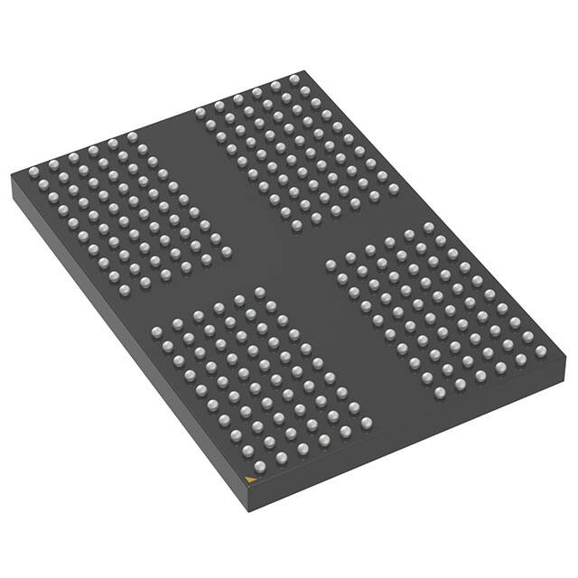
• 200-ball x16/x32 BGA (10x14.5mm)
ADDRESS TABLE *
Parameter
# of Channel
Row Addresses
Column Addresses
Bank Addresses
2
1
R0-R14
R0-R13
C0-C9
BA0-BA2
Note: Address information is per channel base.
KEY TIMING PARAMETERS
Speed
Grade
Freq.
(MHz)
Data
Rate
(Mb/s)
Write
Latency
Read
Latency
Set
Set
DBI
DBI
A
B
OFF
ON
-062
1600
3200
14
26
28
32
-075
1333
2666
12
22
24
28
Note: Other clock frequencies/data rates supported; please
refer to AC timing tables.
Copyright © 2021 Integrated Silicon Solution, Inc. All rights reserved. ISSI reserves the right to make changes to this specification and its products at any time without notice. ISSI assumes no
liability arising out of the application or use of any information, products or services described herein. Customers are advised to obtain the latest version of this device specification before relying on
any published information and before placing orders for products.
Integrated Silicon Solution, Inc. does not recommend the use of any of its products in life support applications where the failure or malfunction of the product can reasonably be expected to cause failure of the life support system or to significantly affect its safety or effectiveness. Products are not authorized for use in such applications unless Integrated Silicon
Solution, Inc. receives written assurance to its satisfaction, that:
a.) the risk of injury or damage has been minimized;
b.) the user assume all such risks; and
c.) potential liability of Integrated Silicon Solution, Inc is adequately protected under the circumstances
Integrated Silicon Solution, Inc. — www.issi.com 1
Rev. A3
08/18/2021
�® Long-term Support
World Class Quality
IS43/46LQ16256A, IS43/46LQ16256AL
IS43/46LQ32128A, IS43/46LQ32128AL
1. BALL ASSIGNMENTS AND DESCRIPTIONS (for x16)
0.65mm Pitch
200-ball x16 Discrete Package, 0.80mm x 0.65mm using MO-311
1
2
3
4
5
A
DNU
DNU
VSS
VDD2
ZQ0
B
DNU
DQ0_A
VDDQ
DQ7_A
C
VSS
DQ1_A
DMI0_A
D
VDDQ
VSS
E
VSS
F
6
7
8
9
10
11
12
NC
VDD2
VSS
DNU
DNU
VDDQ
VDDQ
DQ15_A
VDDQ
DQ8_A
DNU
DQ6_A
VSS
VSS
DQ14_A
DMI1_A
DQ9_A
VSS
DQS0_T_A
VSS
VDDQ
VDDQ
VSS
DQS1_T_A
VSS
VDDQ
DQ2_A
DQS0_C_
A
DQ5_A
VSS
VSS
DQ13_A
VDD1
DQ3_A
VDDQ
DQ4_A
VDD2
VDD2
DQ12_A
VDDQ
DQ11_A
VDD1
G
VSS
ODT_CA_
A
VSS
VDD1
VSS
VSS
VDD1
VSS
NC
VSS
H
VDD2
CA0_A
NC
CS0_A
VDD2
VDD2
CA2_A
CA3_A
CA4_A
VDD2
J
VSS
CA1_A
VSS
CKE0_A
NC
CK_t_A
CK_c_A
VSS
CA5_A
VSS
K
VDD2
VSS
VDD2
VSS
NC
NC
VSS
VDD2
VSS
VDD2
N
VDD2
VSS
VDD2
VSS
NC
NC
VSS
VDD2
VSS
VDD2
P
VSS
NC
VSS
NC
NC
NC
NC
VSS
NC
VSS
R
VDD2
NC
NC
NC
VDD2
VDD2
NC
NC
NC
VDD2
T
VSS
NC
VSS
VDD1
VSS
VSS
VDD1
VSS
RESET_N
VSS
U
VDD1
NC
VDDQ
NC
VDD2
VDD2
NC
VDDQ
NC
VDD1
V
VSS
NC
NC
NC
VSS
VSS
NC
NC
NC
VSS
W
VDDQ
VSS
NC
VSS
VDDQ
VDDQ
VSS
NC
VSS
VDDQ
Y
VSS
NC
NC
NC
VSS
VSS
NC
NC
NC
VSS
AA
DNU
NC
VDDQ
NC
VDDQ
VDDQ
NC
VDDQ
NC
DNU
AB
DNU
DNU
VSS
VDD2
VSS
VSS
VDD2
VSS
DNU
DNU
0.80mm Pitch
DQS1_C_
DQ10_A
A
VSS
L
M
NOTE 1 0.8mm pitch (X-axis), 0.65mm pitch (Y-axis), 22 rows.
NOTE 2 Top View, A1 in top left corner.
NOTE 3 Die pad VSS and VSSQ signals are combined to VSS package balls.
Integrated Silicon Solution, Inc. — www.issi.com 2
Rev. A3
08/18/2021
�® Long-term Support
World Class Quality
IS43/46LQ16256A, IS43/46LQ16256AL
IS43/46LQ32128A, IS43/46LQ32128AL
1. BALL ASSIGNMENTS AND DESCRIPTIONS
0.65mm Pitch
200-ball x32 Discrete Package, 0.80mm x 0.65mm using MO-311
1
2
3
4
5
A
DNU
DNU
VSS
VDD2
ZQ0
B
DNU
DQ0_A
VDDQ
DQ7_A
C
VSS
DQ1_A
DMI0_A
D
VDDQ
VSS
E
VSS
F
6
7
8
9
10
11
12
NC
VDD2
VSS
DNU
DNU
VDDQ
VDDQ
DQ15_A
VDDQ
DQ8_A
DNU
DQ6_A
VSS
VSS
DQ14_A
DMI1_A
DQ9_A
VSS
DQS0_T_A
VSS
VDDQ
VDDQ
VSS
DQS1_T_A
VSS
VDDQ
DQ2_A
DQS0_C_
A
DQ5_A
VSS
VSS
DQ13_A
VDD1
DQ3_A
VDDQ
DQ4_A
VDD2
VDD2
DQ12_A
VDDQ
G
VSS
ODT_CA_
A (3)
VSS
VDD1
VSS
VSS
VDD1
VSS
H
VDD2
CA0_A
NC
CS0_A
VDD2
VDD2
CA2_A
CA3_A
CA4_A
VDD2
J
VSS
CA1_A
VSS
CKE0_A
NC
CK_t_A
CK_c_A
VSS
CA5_A
VSS
K
VDD2
VSS
VDD2
VSS
NC
NC
VSS
VDD2
VSS
VDD2
N
VDD2
VSS
VDD2
VSS
NC
NC
VSS
VDD2
VSS
VDD2
P
VSS
CA1_B
VSS
CKE0_B
NC
CK_T_B
CK_C_B
VSS
CA5_B
VSS
R
VDD2
CA0_B
NC
CS0_B
VDD2
VDD2
CA2_B
CA3_B
CA4_B
VDD2
T
VSS
ODT_CA_
B (3)
VSS
VDD1
VSS
VSS
VDD1
VSS
RESET_N
VSS
U
VDD1
DQ3_B
VDDQ
DQ4_B
VDD2
VDD2
DQ12_B
VDDQ
DQ11_B
VDD1
V
VSS
DQ2_B
DQS0_C_
B
DQ5_B
VSS
VSS
DQ13_B
W
VDDQ
VSS
DQS0_T_B
VSS
VDDQ
VDDQ
VSS
DQS1_T_B
VSS
VDDQ
Y
VSS
DQ1_B
DMI0_B
DQ6_B
VSS
VSS
DQ14_B
DMI1_B
DQ9_B
VSS
AA
DNU
DQ0_B
VDDQ
DQ7_B
VDDQ
VDDQ
DQ15_B
VDDQ
DQ8_B
DNU
AB
DNU
DNU
VSS
VDD2
VSS
VSS
VDD2
VSS
DNU
DNU
0.80mm Pitch
DQS1_C_
DQ10_A
A
DQ11_A
NC
VSS
VDD1
VSS
L
M
DQS1_C_
DQ10_B
B
VSS
NOTE 1 0.8mm pitch (X-axis), 0.65mm pitch (Y-axis), 22 rows.
NOTE 2 Top View, A1 in top left corner.
NOTE 3 The ODT_CA pin is ignored by LPDDR4X devices.
Integrated Silicon Solution, Inc. — www.issi.com 3
Rev. A3
08/18/2021
�IS43/46LQ16256A, IS43/46LQ16256AL
IS43/46LQ32128A, IS43/46LQ32128AL
® Long-term Support
World Class Quality
2. INPUT/OUTPUT FUNTIONAL DESCRIPTION
2.1 PAD DEFINITION AND DESCRIPTION
Table 2.1 — Pad Definition and Description
Symbol
Type
CK_t_A,
CK_c_A,
CK_t_B,
CK_c_B
Input
Description
Clock: CK_t and CK_c are differential clock inputs. All address, command,
and control input signals are sampled on the crossing of the positive edge of
CK_t and the negative edge of CK_c. AC timings for CA parameters are
referenced to CK. Each channel (A & B) has its own clock pair.
Clock Enable: CKE HIGH activates and CKE LOW deactivates the internal
clock circuits, input buffers, and output drivers. Power-saving modes are
entered and exited via CKE transitions. CKE is part of the command code.
Each channel (A & B) has its own CKE signal.
CKE_A
CKE_B
Input
CS_A
CS_B
Input
CA[5:0]_A
CA[5:0]_B
Input
ODT_CA_A
ODT_CA_B
Input
DQ[15:0]_A,
DQ[15:0]_B
I/O
Data Input/Output: Bi-direction data bus.
I/O
Data Strobe: DQS_t and DQS_c are bi-directional differential output clock
signals used to strobe data during a READ or WRITE. The Data Strobe is
generated by the DRAM for a READ and is edge-aligned with Data. The Data
Strobe is generated by the Memory Controller for a WRITE and must arrive
prior to Data. Each byte of data has a Data Strobe signal pair. Each channel
(A & B) has its own DQS strobes.
I/O
Data Mask Inversion: DMI is a bi-directional signal which is driven HIGH
when the data on the data bus is inverted, or driven LOW when the data is in
its normal state. Data Inversion can be disabled via a mode register setting.
Each byte of data has a DMI signal. Each channel (A & B) has its own DMI
signals.
DQS[1:0]_t_A,
DQS[1:0]_c_A,
DQS[1:0]_t_B,
DQS[1:0]_c_B
DMI[1:0]_A,
DMI[1:0]_B
ZQ
Reference
Chip Select: CS is part of the command code. Each channel (A & B) has its
own CS signal.
Command/Address Inputs: CA signals provide the Command and Address
inputs according to Table 63 — Command Truth Table. Each channel (A&B)
has its own CA signals.
LPDDR4 CA ODT Control: The ODT_CA pin is used in conjunction with the
Mode Register to turn on/off the On-Die-Termination for CA pins.
LPDDR4X CA ODT Control: The ODT_CA pin is ignored by LPDDR4X
devices. CA ODT is fully controlled through MR11 and MR22. The ODT_CA
pin shall be connected to either VDD2 or VSS.
Calibration Reference: Used to calibrate the output drive strength and the
termination resistance. There is one ZQ pin per die. The ZQ pin shall be
connected to VDDQ through a 240Ω ± 1% resistor.
VDDQ,
VDD1,
Supply
VDD2
VSS, VSSQ
GND
Ground Reference: Power supply ground reference
RESET_n
Input
RESET: When asserted LOW, the RESET_n signal resets both channels of
the die.
Power Supplies: Isolated on the die for improved noise immunity.
Integrated Silicon Solution, Inc. — www.issi.com 4
Rev. A3
08/18/2021
�IS43/46LQ16256A, IS43/46LQ16256AL
IS43/46LQ32128A, IS43/46LQ32128AL
® Long-term Support
World Class Quality
ORDERING INFORMATION – Valid Part Numbers
IS 43 LQ 32128
A
- 062 B L I
TEMPERATURE RANGE
I = Industrial (-40°C to +95°C)
A1 = Automotive A1 Grade (-40°C to +95°C)
A2 = Automotive A2 Grade (-40°C to +105°C)
A3 = Automotive A3 Grade (-40°C to +125°C)
PACKAGING CONTENT
L = RoHS compliant
Package Type
B = 200-ball BGA (0.85mm max thickness)
TB = 200-ball BGA (1.1mm max thickness)
Speed Grade
075 = 1333MHz
062 = 1600MHz
VDDQ
Blank = Regular VDDQ (LPDDR4)
L = Low VDDQ (LPDDR4X)
Die Generation
A = 1st Generation
ECC support
Blank = No ECC Support
Density
16256 = 256Mb x 16 (4Gb)
32128 = 128Mb x 32 (4Gb)
Device Type
LQ = LPDDR4 DRAM
Product Family
43 = DDR DRAM
46 = Automotive DDR DRAM
ISSI Prefix
IS = Integrated Silicon Solution Inc.
Integrated Silicon Solution, Inc. — www.issi.com 5
Rev. A3
08/18/2021
�® Long-term Support
World Class Quality
IS43/46LQ16256A, IS43/46LQ16256AL
IS43/46LQ32128A, IS43/46LQ32128AL
ORDERING INFORMATION, 256Mb x 16 LPDDR4
256Mb x 16 - Industrial Range: Tc = -40°C to +95°C
Clock
Speed Grade
1600 MHz
-062
Order Part No.
Package
IS43LQ16256A-062BLI
200 ball FBGA, lead free
IS43LQ16256A-062TBLI
200 ball FBGA, lead free
256Mb x 16 - Automotive, A1 Range: Tc = -40°C to +95°C
Clock
Speed Grade
1600 MHz
-062
Order Part No.
Package
IS46LQ16256A-062BLA1
200 ball FBGA, lead free
IS46LQ16256A-062TBLA1
200 ball FBGA, lead free
256Mb x 16 - Automotive, A2 Range: Tc = -40°C to +105°C
Clock
1600 MHz
Speed Grade
-062
Order Part No.
Package
IS46LQ16256A-062BLA2
200 ball FBGA, lead free
IS46LQ16256A-062TBLA2
200 ball FBGA, lead free
256Mb x 16 - Automotive, A3 Range: Tc = -40°C to +125°C
Clock
Speed Grade
1600 MHz
-062
Order Part No.
Package
IS46LQ16256A-062BLA3
200 ball FBGA, lead free
IS46LQ16256A-062TBLA3
200 ball FBGA, lead free
Integrated Silicon Solution, Inc. — www.issi.com 6
Rev. A3
08/18/2021
�® Long-term Support
World Class Quality
IS43/46LQ16256A, IS43/46LQ16256AL
IS43/46LQ32128A, IS43/46LQ32128AL
ORDERING INFORMATION, 256Mb x 16 LPDDR4X
256Mb x 16 - Industrial Range: Tc = -40°C to +95°C
Clock
Speed Grade
1600 MHz
-062
Order Part No.
Package
IS43LQ16256AL-062BLI
200 ball FBGA, lead free
IS43LQ16256AL-062TBLI
200 ball FBGA, lead free
256Mb x 16 - Automotive, A1 Range: Tc = -40°C to +95°C
Clock
1600 MHz
Speed Grade
-062
Order Part No.
Package
IS46LQ16256AL-062BLA1
200 ball FBGA, lead free
IS46LQ16256AL-062TBLA1
200 ball FBGA, lead free
256Mb x 16 - Automotive, A2 Range: Tc = -40°C to +105°C
Clock
Speed Grade
1600 MHz
-062
Order Part No.
Package
IS46LQ16256AL-062BLA2
200 ball FBGA, lead free
IS46LQ16256AL-062TBLA2
200 ball FBGA, lead free
256Mb x 16 - Automotive, A3 Range: Tc = -40°C to +125°C
Clock
Speed Grade
1600 MHz
-062
Order Part No.
Package
IS46LQ16256AL-062BLA3
200 ball FBGA, lead free
IS46LQ16256AL-062TBLA3
200 ball FBGA, lead free
Integrated Silicon Solution, Inc. — www.issi.com 7
Rev. A3
08/18/2021
�® Long-term Support
World Class Quality
IS43/46LQ16256A, IS43/46LQ16256AL
IS43/46LQ32128A, IS43/46LQ32128AL
ORDERING INFORMATION, 128Mb x 32 LPDDR4
128Mb x 32 - Industrial Range: Tc = -40°C to +95°C
Clock
1600 MHz
Speed Grade
-062
Order Part No.
Package
IS43LQ32128A-062BLI
200 ball FBGA, lead free
IS43LQ32128A-062TBLI
200 ball FBGA, lead free
128Mb x 32 - Automotive, A1 Range: Tc = -40°C to +95°C
Clock
Speed Grade
1600 MHz
-062
Order Part No.
Package
IS46LQ32128A-062BLA1
200 ball FBGA, lead free
IS46LQ32128A-062TBLA1
200 ball FBGA, lead free
128Mb x 32 - Automotive, A2 Range: Tc = -40°C to +105°C
Clock
Speed Grade
Order Part No.
Package
1333 MHz
-075
IS46LQ32128A-075BLA2
IS46LQ32128A-062BLA2
200 ball FBGA, lead free
200 ball FBGA, lead free
IS46LQ32128A-062TBLA2
200 ball FBGA, lead free
1600 MHz
-062
128Mb x 32 - Automotive, A3 Range: Tc = -40°C to +125°C
Clock
1600 MHz
Speed Grade
-062
Order Part No.
Package
IS46LQ32128A-062BLA3
200 ball FBGA, lead free
IS46LQ32128A-062TBLA3
200 ball FBGA, lead free
Integrated Silicon Solution, Inc. — www.issi.com 8
Rev. A3
08/18/2021
�® Long-term Support
World Class Quality
IS43/46LQ16256A, IS43/46LQ16256AL
IS43/46LQ32128A, IS43/46LQ32128AL
ORDERING INFORMATION, 128Mb x 32 LPDDR4X
128Mb x 32 - Industrial Range: Tc = -40°C to +95°C
Clock
Speed Grade
1600 MHz
-062
Order Part No.
Package
IS43LQ32128AL-062BLI
200 ball FBGA, lead free
IS43LQ32128AL-062TBLI
200 ball FBGA, lead free
128Mb x 32 - Automotive, A1 Range: Tc = -40°C to +95°C
Clock
Speed Grade
1600 MHz
-062
Order Part No.
Package
IS46LQ32128AL-062BLA1
200 ball FBGA, lead free
IS46LQ32128AL-062TBLA1
200 ball FBGA, lead free
128Mb x 32 - Automotive, A2 Range: Tc = -40°C to +105°C
Clock
Speed Grade
1600 MHz
-062
Order Part No.
Package
IS46LQ32128AL-062BLA2
200 ball FBGA, lead free
IS46LQ32128AL-062TBLA2
200 ball FBGA, lead free
128Mb x 32 - Automotive, A3 Range: Tc = -40°C to +125°C
Clock
Speed Grade
1600 MHz
-062
Order Part No.
Package
IS46LQ32128AL-062BLA3
200 ball FBGA, lead free
IS46LQ32128AL-062TBLA3
200 ball FBGA, lead free
Integrated Silicon Solution, Inc. — www.issi.com 9
Rev. A3
08/18/2021
�IS43/46LQ16256A, IS43/46LQ16256AL
IS43/46LQ32128A, IS43/46LQ32128AL
® Long-term Support
World Class Quality
PACKAGE INFORMATION: 200-ball FBGA
Package Outline
10/29/2020
Integrated Silicon Solution, Inc. — www.issi.com 10
Rev. A3
08/18/2021
�IS43/46LQ16256A, IS43/46LQ16256AL
IS43/46LQ32128A, IS43/46LQ32128AL
® Long-term Support
World Class Quality
Package Outline
5/18/2020
Integrated Silicon Solution, Inc. — www.issi.com 11
Rev. A3
08/18/2021
�


 工商网监
湘ICP备2023018690号
工商网监
湘ICP备2023018690号

