IS43R32800B
8Mx32
256Mb DDR Synchronous DRAM
FEATURES
• Vdd/Vddq=2.5V+0.2V (-5, -6, -75)
• Double data rate architecture; two data transfers
per clock cycle
• Bidirectional, data strobe (DQS) is transmitted/
received with data
• Differential clock input (CLK and /CLK)
• DLL aligns DQ and DQS transitions with CLK
transitions edges of DQS
• Commands entered on each positive CLK edge;
• Data and data mask referenced to both edges of
DQS
• 4 bank operation controlled by BA0, BA1 (Bank
Address)
• /CAS latency –2.0/2.5/3.0 (programmable)
• Burst length - 2/4/8 (programmable)
• Burst type - Sequential/ Interleave (programmable)
• Auto precharge / All bank precharge controlled
by A8
• 4096 refresh cycles/ 64ms (4 banks concurrent
refresh)
• Auto refresh and Self refresh
• Row address A0-11/ Column address A0-7, A9SSTL_2 Interface
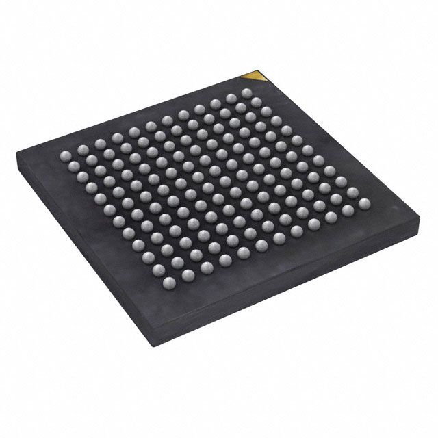
• Package 144-ball FBGA
• Available in Industrial Temperature
• Temperature Range:
Commercial (0oC to +70oC)
Industrial (-40oC to +85oC)
PRELIMINARY INFORMATION
MAY 2008
DESCRIPTION:
IS43R32800B is a 4-bank x 2,097,152-word x32bit
Double Data Rate Synchronous DRAM, with SSTL_2
interface. All control and address signals are referenced
to the rising edge of CLK. Input data is registered on
both edges of data strobe, and output data and data
strobe are referenced on both edges of CLK. The
IS43R32800B achieves very high speed clock rate up to
200 MHz. It is packaged in 144-ball FBGA.
KEY TIMING PARAMETERS
Parameter
-5
-6
-75 Unit
Clk Cycle Time
CAS Latency = 3
5
6
7.5 ns
CAS Latency = 2.5
5
6
7.5 ns
CAS Latency = 2
7.5
7.5
7.5 ns
Clk Frequency
CAS Latency = 3
200
167 143 MHz
CAS Latency = 2.5 200
167 143 MHz
CAS Latency = 2
143
143 143 MHz
Access Time from Clock
CAS Latency = 3
+0.70 +0.70 +0.70 ns
CAS Latency = 2.5 +0.70 +0.70 +0.70 ns
CAS Latency = 2
+0.75 +0.75 +0.70 ns
ADDRESS TABLE
Parameter
8M x 32
Configuration
2M x 32 x 4 banks
Bank Address Pins
BA0, BA1
Autoprecharge Pins
A8/AP
Row Addresses
A0 – A11
Column Addresses
A0 – A7, A9
Refresh Count
4096 / 64ms
Copyright © 2006 Integrated Silicon Solution, Inc. All rights reserved. ISSI reserves the right to make changes to this specification and its products at any time without
notice. ISSI assumes no liability arising out of the application or use of any information, products or services described herein. Customers are advised to obtain the latest version of this device specification before relying on any published information and before placing orders for products.
Integrated Silicon Solution, Inc. — www.issi.com
Rev. 00D
03/19/08
1
�IS43R32800B
FUNCTIONAL BLOCK DIAGRAM
DLL
Memory
Array
Ba nk #0
DQ 0 - 31
DQS0 - 3
I/O Buffer
DQ S B uffer
Memory
Array
Ba nk #1
Memory
Array
Ba nk #2
Memory
Array
Ba nk #3
Mode Re gister
Control C ircu itry
Addres s B uffer
Control Signal B uffer
Cl ock B uffer
A0-1 1
/CS /RAS /CAS
BA 0,1
CLK
2
/CLK
/WE
D M0- 3
CKE
Integrated Silicon Solution, Inc. — www.issi.com
Rev. 00D
03/19/08
�IS43R32800B
PIN CONFIGURATION
Package Code: B 144-ball FBGA (Top View) (12.00mm x 12.00mm Body, 0.8mm Ball Pitch
1
2
3
4
5
6
7
8
9
10
11
12
A
DQS0
DM0
VSSQ
DQ 3
DQ 2
DQ 0
DQ 31
DQ 29
DQ 28
VSSQ
DM3
DQS3
B
DQ 4
VDDQ
NC
VDDQ
DQ 1
VDDQ
VDDQ
DQ 30
VDDQ
NC
VDDQ
DQ 27
C
DQ 6
DQ 5
VSSQ
VSSQ
VSSQ
VD D
VD D
VSSQ
VSSQ
VSSQ
DQ 26
DQ 25
D
DQ 7
VDDQ
VD D
VSS
VSSQ
VSS
VSS
VSSQ
VSS
VD D
VDDQ
DQ 24
E
DQ 17
DQ 16
VDDQ
VSSQ
VSS
VSS
VSS
VSS
VSSQ
VDDQ
DQ 15
DQ 14
F
DQ 19
DQ 18
VDDQ
VSSQ
VSS
VSS
VSS
VSS
VSSQ
VDDQ
DQ 13
DQ 12
G
DQS2
DM2
NC
VSSQ
VSS
VSS
VSS
VSS
VSSQ
NC
DM1
DQS1
H
DQ 21
DQ 20
VDDQ
VSSQ
VSS
VSS
VSS
VSS
VSSQ
VDDQ
DQ 11
DQ 10
J
DQ 22
DQ 23
VDDQ
VSSQ
VSS
VSS
VSS
VSS
VSSQ
VDDQ
DQ 9
DQ 8
K
/CAS
/W E
VD D
VSS
A1 0
VD D
VD D
NC
VSS
VD D
NC
NC
L
/R AS
NC
NC
BA 1
A2
A1 1
A9
A5
NC
CL K
/CLK
NC
M
/CS
NC
BA 0
A0
A1
A3
A4
A6
A7
A8 /AP
CK E
VREF
PIN DESCRIPTIONS
CLK, /CLK
CKE
/CS
/RAS
/CAS
/WE
DQ 0-31
DM 0-3
: Ma ster Cl ock
: Clock En able
: Ch ip Select
: Ro w Address Strobe
: Column A ddress Strobe
: Write Enab le
: Data I/O
: Write Mask
Integrated Silicon Solution, Inc. — www.issi.com
Rev. 00D
03/19/08
A0-11
BA 0,1
VDD
VDDQ
Vs s
VssQ
DQ S0-3
VREF
: Address Inpu t
: Ba nk A ddress Inpu t
: Pow er Supply
: Power Supply for Output
: Ground
: Ground for Output
: Data Strobe
: Reference Voltage
3
�IS43R32800B
PIN FUNCTIONS
SYMBOL
DESCRIPTION
Input
Cl ock: CL K a nd/CLK are differential clock inputs. A ll address and control
input signals are sampled on the crossing of the positive edge of CL K a nd
negative edgeof /CLK . Output (read) data is referenced to the crossings of
CL K a nd /CLK (both directions of crossing).
CK E
I nput
Cl ock E nable: CK E controls internal clock. W hen CKE is low, internal clock
for the following cycle is ceased. C KE is also used to select auto/ self refresh.
Af ter self refresh mode is started, CK E becomes asynchronous input. Self refresh
is maintained as long as CK E i s low.
/CS
I nput
Chip Select: W hen /CS is high, any command means No Operation.
/RAS , /CAS, /WE
I nput
Combination of /RA S, /CAS , /WE defines basic commands.
CL K, /CLK
A0-1 1 specify the Row / Column Address in conjunction with BA0,1. T he
Row Address is specifi ed by A0-11. The Column Address is specified by
A0-7 ,A 9. A8 is also used to indicate precharge option. W hen A8 is
high at a read / write command, an auto precharge is performed. When A8
is high at a precharge command, all banks are precharged.
A0-1 1
Input
BA 0,1
Input
DQ0-31
Input / Output
Data Input/Output: D ata bus
Input / Output
Data Strobe: Outputwith read data, inputwith write data. E dge-aligned
with read data, centered in write data. Used to capture write data.
DQS 0 for DQ0 - DQ7, DQS 1 for DQ8 - DQ15, DQS2 for DQ16 - DQ23,
DQS3 for DQ24 - DQ31.
DQS0- 3
DM0- 3
Input
VDD, Vs s
Power Supply
VDDQ , VssQ
Vref
4
TYPE
Power Supply
Input
Bank Address: BA 0,1 specifies one of four banks to which a command is
applied. BA 0,1 must be set with ACT, PR E, READ, WR IT E commands.
Input Data Mask: DM is an inputmask signal for write data. I nput data
is masked when DM is sampled HIG H along with that input data
during a WR IT E access. DM is sampled on both edges of D QS.
Al though DM pins are input only, the DM loading matches the DQ
andDQS loading. DM 0 for DQ0 - DQ7, DM1 for DQ8 - DQ15,
DM 2 for DQ16 - DQ23, DM 3 for DQ24 - DQ31.
Power Supply for the memory array and peripheral circuitry.
VDDQ and VssQ are supplied to the Output Buffers only.
SST L_ 2 reference voltage.
Integrated Silicon Solution, Inc. — www.issi.com
Rev. 00D
03/19/08
�IS43R32800B
FUNCTIONAL DESCRIPTION
ISSI's 256-Mbit DDR SDRAM provides basic functions, bank (row) activate, burst read / write, bank (row)
precharge, and auto / self refresh. E ach command is defined by control signals of /RA S, /CAS and
/WE at CLK rising edge. I n addition to 3 signals, /CS ,C KE and A8 are usedas chip select, refresh
option, and prechargeoption, respectively. To know the detailed definition of commands, please
see the command truth table.
/CLK
CL K
/CS
Chip Select : L =select, H=deselect
/RAS
Command
/CAS
Command
/WE
Command
CK E
Refresh Option @ refresh command
A8
Precharge Option @ precharge or read/write command
define basic commands
Activate ( ACT) [/RA S =L, /CAS =/WE =H ]
AC T c ommand activates a row in an idle bank indicated by BA .
Read (R EAD) [/RAS =H , /CA S =L, /WE = H]
RE AD command starts burst read from the active bank indicated by BA . F irst output data appears after
/CAS latency. When A8 =H at this command, the bank is deactivated after the burst read (autoprecharge READ A )
Write (WRITE) [/RA S =H, /CAS =/WE =L ]
WR IT E c ommand starts burst write to the active bank indicated by BA . T otal data length to be written
is set by burst length. W hen A8 =H at this command, the bank is deactivated after the burst write
(auto-precharge, WRITEA )
Prechar ge (P RE ) [ /RAS =L , /CA S =H, /WE = L]
PR E c ommand deactivates the active bank indicated by BA . T his command also terminates burst read
/write operation. When A8 =H at this command, all banks are deactivated (precharge all, PREA ).
Auto-Ref resh (REFA ) [ /RAS =/CA S =L, /WE = CK E = H]
RE FA command starts auto-refresh cycle. R efresh address including bank address are generated
internally. A fter this command, the banks are precharged automatically.
Integrated Silicon Solution, Inc. — www.issi.com
Rev. 00D
03/19/08
5
�IS43R32800B
COMMAND TRUTH TABLE
MNEMONIC
CKE
n-1
CKE
n
/CS
/RAS
/CAS
DESEL
H
X
H
X
X
X
X
X
X
No Operation
NOP
H
X
L
H
H
H
X
X
X
Row Address Entry &
Bank Activate
ACT
H
H
L
L
H
H
V
V
V
Single Bank Precharge
PRE
H
H
L
L
H
L
V
L
X
PrechargeAll Banks
PREA
H
H
L
L
H
L
X
H
X
Column Address Entry
& Write
WRITE
H
H
L
H
L
L
V
L
V
Column Address Entry
& Write with
Auto-Precharge
WRITEA
H
H
L
H
L
L
V
H
V
Column Address Entry
& Read
READ
H
H
L
H
L
H
V
L
V
Column Address Entry
& Read with
Auto-Precharge
READA
H
H
L
H
L
H
V
H
V
Auto-Refresh
REFA
H
H
L
L
L
H
X
X
X
Self-RefreshEntry
REFS
H
L
L
L
L
H
X
X
X
Self-RefreshExit
REFSX
L
H
H
X
X
X
X
X
X
L
H
L
H
H
H
X
X
X
Burst Terminate
TERM
H
H
L
H
H
L
X
X
X
1
ModeRegisterSet
MRS
H
H
L
L
L
L
L
L
V
2
COMMAND
Deselect
/WE BA0,1
A8
/AP
A0-7,
note
A9-11
H=High Level, L=Low Level, V=Valid, X=Don't Care, n=CLK cycle number
NOTE:
1. Applies only to read bursts with autoprecharge disabled; this command is undefi ned (and should not be used) for
read bursts wi th autoprecharge enabled, and for write bursts.
2. BA 0-BA 1 select either the Baseor the Extended Mode Register (BA 0 = 0, BA 1 = 0 selects Mode Register;BA0=1 ,
BA 1 = 0 selects Extended Mode Register; other combinations of BA 0-BA 1 are reserved; A 0-A11 provide the
op-code to be written to the selected Mode Register.
6
Integrated Silicon Solution, Inc. — www.issi.com
Rev. 00D
03/19/08
�IS43R32800B
FUNCTIONAL TRUTH TABLE
Current State
IDLE
ROW A CT IV E
RE AD(Au toPrecharge
Disabled)
/CS /RAS /CAS /WE Address
H
X
X
X X
C ommand
D ES EL
Action
NO P
L
L
H
H
H
H
H
L
X
BA
N OP
TERM
NO P
ILLE GAL
L
L
L
H
L
L
L
H
H
X
H
L
BA , C A, A8
BA , R A
BA , A 8
RE AD / WRITE
A CT
PRE / PRE A
ILLEGAL
Bank Active, L atch RA
N OP
2
L
L
L
H
R EF A
A uto-Refresh
5
L
L
L
MR S
M ode Register Set
5
H
L
L
X
H
H
X
H
H
X
Op-C ode, ModeL
Add
X X
H X
L BA
DE SE L
NOP
TER M
L
H
L
H
BA , C A, A8
RE AD / READA
L
H
L
L
BA , C A, A8
WR ITE / WR ITEA
L
L
H
H
BA , R A
A CT
N OP
NO P
I LLEGA L
Begin Read, L atch CA , Determine
Auto-Precharge
Begin Write, L atch CA , Determine
Auto-Precharge
Bank Active / ILLEG AL
2
L
L
L
L
H
L
L
H
PRE / PRE A
R EF A
P recharge / Precharge All
I LLE GA L
L
L
L
L
MR S
I LLE GA L
H
L
X
H
X
H
X
H
BA , A 8
X
Op-C ode, ModeAdd
X
X
D ES EL
NOP
NOP (C ontinueBurst to END)
NO P (Continue Burst to END)
L
H
H
L
BA
TER M
L
H
L
H
BA , C A, A8
RE AD / REA DA
L
H
L
L
BA , C A, A8
WR IT E / WR ITEA
T erminate Burst
Terminate Burst, L atch CA , B egin
New Read, Determine AutoPrecharge
ILLE GA L
L
L
L
L
H
H
H
L
BA , R A
BA , A 8
A CT
PRE / PRE A
Bank Active / ILLE GAL
T erminate Burst, Precharge
L
L
L
H
L
L
L
L
X
REF A
Op-C ode, ModeMR S
Add
Integrated Silicon Solution, Inc. — www.issi.com
Rev. 00D
03/19/08
Notes
2
4
3
2
I LLE GAL
I LLE GAL
7
�IS43R32800B
FUNCTIONAL TRUTH TABLE (continued)
Current State
WR IT E( AutoPrecharge
Disabled)
READ with
Auto-Precharge
WRITE with
Auto-Precharge
8
/CS /RAS /CAS /WE Addres s
H
X
X
X X
L
H
H
H X
Command
DES EL
NOP
Action
NO P (Continue Burst to END)
NO P (Continue Burst to END)
Notes
L
H
H
L
BA
TERM
L
H
L
H
BA , C A, A8
READ / READA
L
H
L
L
BA , C A, A8
WR ITE / WR IT EA
L
L
H
H
BA , R A
ACT
IL LE GAL
Terminate Burst, L atchCA , B egin
Read, Determine Auto-Precharge
Terminate Burst, L atchCA , B egin
Write, Determine Auto-Precharge
Bank Active / ILLE GAL
L
L
H
L
BA , A 8
PRE / PRE A
T erminate Burst, Precharge
L
L
L
H
I LL EGAL
L
L
L
L
H
X
X
X
X
REF A
Op-C ode, ModeMR S
Add
X
DES EL
L
H
H
H
X
NOP
NO P (Continue Burst to END)
L
L
L
L
L
H
H
H
L
L
H
L
L
H
H
L
H
L
H
L
BA
BA , C A, A8
BA , C A, A8
BA , R A
BA , A 8
TERM
READ / READA
WRIT E / WR IT EA
ACT
PRE / PRE A
ILLE GAL
ILLE GAL
IL LE GAL
Bank Active / ILLE GAL
P recharge / ILLEGAL
L
L
L
H
I LLEGAL
L
L
L
L
H
X
X
X
X
REF A
Op-C ode, M odeMR S
Add
X
DES EL
L
L
L
L
L
H
H
H
H
L
H
H
L
L
H
H
L
H
L
H
X
BA
BA , C A, A8
BA , C A, A8
BA , R A
NOP
TERM
READ / READA
WR IT E / WR ITEA
A CT
NOP (Continue Burst to END)
ILLE GAL
ILLEGAL
ILLE GAL
Bank Active / ILLEGAL
2
L
L
H
L
BA , A 8
PRE / PRE A
P recharge / ILLEGAL
2
L
L
L
H
L
L
L
L
X
REF A
Op-C ode, ModeMRS
Add
3
3
2
I LL EGAL
NO P (Continue Burst to END)
2
2
I LLEGAL
NOP (Continue Burst to END)
I LLEGAL
I LLEGAL
Integrated Silicon Solution, Inc. — www.issi.com
Rev. 00D
03/19/08
�IS43R32800B
FUNCTIONAL TRUTH TABLE (continued)
Current State
PR EC HARGI NG
ROW
ACTI VATING
WRITER ECOVERING
/CS /RAS /CAS /W E Address
H
X
X
X X
Action
NOP (I dle after tRP)
L
H
H
H
X
NOP
NOP (I dle after tRP)
L
L
L
H
H
L
H
L
H
L
X
H
BA
BA , C A, A8
BA , R A
TERM
READ / WRITE
A CT
IL LEG AL
IL LEG AL
IL LE GA L
PRE / PRE A
L
L
H
L
BA , A 8
L
L
L
H
I LLEGAL
L
L
L
L
H
X
X
X
X
REF A
Op-C ode, M odeMRS
Add
X
DES EL
L
H
H
H
X
NOP
NOP (R ow Active after tRC D)
L
L
L
H
H
L
H
L
H
L
X
H
BA
BA , C A, A8
BA , R A
TERM
READ / WRITE
ACT
IL LEG AL
IL LEG AL
IL LE GA L
NOP (I dle after tRP)
PRE / PRE A
I LLEG AL
Notes
2
2
2
4
I LLEGAL
NOP (R ow Active after tRC D)
2
2
2
2
L
L
H
L
BA , A 8
L
L
L
H
I LLEG AL
L
L
L
L
H
X
X
X
X
REF A
Op-C ode, M odeMR S
Add
X
DESEL
L
H
H
H
X
NOP
NOP
L
L
L
H
H
L
H
L
H
L
X
H
BA
BA , C A, A8
BA , R A
TERM
READ / WRITE
ACT
IL LE GA L
IL LE GA L
IL LEGA L
2
2
2
PRE / PRE A
I LLEGAL
2
L
L
H
L
BA , A 8
L
L
L
H
L
L
L
L
X
REF A
Op-C ode, M odeMRS
Add
Integrated Silicon Solution, Inc. — www.issi.com
Rev. 00D
03/19/08
Command
DES EL
I LLEGAL
NOP
I LLEGAL
I LLEGA L
9
�IS43R32800B
FUNCTIONAL TRUTH TABLE (continued)
Current State
REFRESHING
MODE
REGISTER
SETTING
/ CS /RAS /C AS /WE Address
H
X
X
X
X
Command
DES EL
Action
NO P (Idle after tRC )
NOP
TERM
READ / WRI TE
ACT
PRE / PRE A
NO P (Idle after tRC )
ILLE GAL
ILLEGAL
ILLEGAL
ILLEG AL
L
L
L
L
L
H
H
H
L
L
H
H
L
H
H
H
L
X
H
L
X
BA
BA , C A, A8
BA , R A
BA , A 8
L
L
L
H
L
L
L
L
H
X
X
X
X
REF A
Op-C ode, ModeMRS
Add
X
DES EL
NO P (Row Active after tRSC )
L
L
L
L
L
H
H
H
L
L
H
H
L
H
H
H
L
X
H
L
X
BA
BA , C A, A8
BA , R A
BA , A 8
NO P (Row Active after tRSC )
ILLEGAL
ILLEGAL
ILLEGAL
ILLEGAL
L
L
L
H
L
L
L
L
X
REF A
Op-C ode, M odeMR S
Add
Notes
ILLEGAL
ILLEGAL
NOP
TERM
READ / WRI TE
ACT
PRE / PRE A
ILLEG AL
ILLEG AL
ABBREVIATIONS :
H=Hi gh Level, L= Low L evel, X =Don't Care
BA =Bank A ddress, R A=Row A ddress, CA =Column Address, NOP =No Operation
NO TES :
1. Al l entries assume that CK E was Hi gh during the preceding clock cycle and the current clock cycle.
2. ILLEGAL to bank in specified state; function may be legal in the bank indicated by B A, depending on the state of
that bank.
3. Must satisfy bus contention, bus turn around, write recovery requirements.
4. NOP to bank precharging or in idle state. May precharge bank indicated by B A.
5. ILLE GAL if any bank is not idle.
ILLE GA L = Device operation and/or data-integrity are not guaranteed.
10
Integrated Silicon Solution, Inc. — www.issi.com
Rev. 00D
03/19/08
�IS43R32800B
CKE TRUTH TABLE
Current State
SELF REFR ESHI NG
POWER
DOWN
ALL BANKS
IDLE
ANY STATE
other than listed
above
CKE n-1
CKE n
/CS
/RAS
/CAS
/WE
Address
A ction
Notes
H
X
X
X
X
X
X
I NV ALID
1
L
H
H
X
X
X
X
Exit Self-Refresh (Idle after tRC )
1
L
H
L
H
H
H
X
Exit Self-Refresh (Idle after tRC )
1
L
H
L
H
H
L
X
I LL EGAL
1
L
H
L
H
L
X
X
I LL EGAL
1
L
H
L
L
X
X
X
I LL EGAL
1
L
L
X
X
X
X
X
N OP (M aintain Self- Refresh)
1
H
X
X
X
X
X
X
I NV AL ID
L
H
X
X
X
X
X
Exit Power Downto Idle
L
L
X
X
X
X
X
N OP (M aintain Self- Refresh)
H
H
X
X
X
X
X
R efer to FunctionTruth Table
2
H
L
L
L
L
H
X
Enter Self-R efresh
2
H
L
H
X
X
X
X
Enter Power Down
2
H
L
L
H
H
H
X
Enter Power Down
2
H
L
L
H
H
L
X
I LL EGAL
2
H
L
L
H
L
X
X
I LL EGAL
2
H
L
L
L
X
X
X
I LL EG AL
2
L
X
X
X
X
X
X
R efer to Current State =Power Down
2
H
H
X
X
X
X
X
R efer to FunctionTruth Table
H
L
X
X
X
X
X
B egin CL K S uspend at Next Cycle
3
L
H
X
X
X
X
X
Exit CLK Suspend at Next Cycle
3
L
L
X
X
X
X
X
M aintain CLK Suspend
ABBR EVIATI ONS :
H=Hi gh Level, L= Low L evel, X =Don't Care
NO TES :
1. CKE L ow to Hi gh transition will re-enable CLK and other inputs asynchronously.
A minimum setup time must be satisfied before any command other than EXIT.
2. Power-Down and Self-Refresh can be entered only from the Al l B anks Idle State.
3. Must be legal command.
Integrated Silicon Solution, Inc. — www.issi.com
Rev. 00D
03/19/08
11
�IS43R32800B
STATE DIAGRAM
POWE R
AP PL IE D
POWER
ON
PR E
CH AR GE
AL L
PREA
SE LF
RE FR ES H
REFS
MR S
MODE
REGISTER
SE T
REFSX
MR S
AU TO
RE FR ES H
REFA
ID LE
CKEL
CKEH
Active
Power
Down
AC T
POWER
DOW N
CKEL
CKEH
RO W
AC TI VE
WR IT E
BU RS T
ST OP
WR IT E
RE AD
WR IT EA
WR IT E
RE AD A
RE AD
WR IT EA
RE AD
RE AD
TE RM
RE AD A
RE AD A
WR IT EA
RE ADA
PR E
PR E
PR E
PR E
CH AR GE
Automatic Sequence
Command Sequence
12
Integrated Silicon Solution, Inc. — www.issi.com
Rev. 00D
03/19/08
�IS43R32800B
ABSOLUTE MAXIMUM RATINGS
Symbol
Parameter
Conditions
R atings
Unit
VDD
Supply V oltage
with respect to V ss
-0.5 ~ 3.7
V
VDDQ
Supply Voltage for Output
with respect to V ssQ
-0.5 ~ 3.7
V
VI
Input V oltage
with respect to V ss
-0.5 ~ V dd+0.5
V
VO
Output Voltage
with respect to Vs sQ
-0.5 ~ V ddQ+0.5
V
IO
Output Current
50
mA
Pd
Power Dissipation
2000
mW
T opr
Operating Temperature
Ts tg
Storage Temperature
5
o
Ta = 25 C
Commercial
Industrial
0 to +70
-40 to +85
o
-65 ~ 150
o
C
C
DC OPERATING CONDITIONS
Parameter
Limits
Unit
Not es
Min.
Typ.
Max.
Supply Voltage
2.3
2.5
2.7
V
-5, -6, -75
Supply Voltage for Output
2.3
2.5
2.7
V
-5, -6, -75
VREF +0.15
V DD+0.3
-0.3
VREF -0.15
V
V
-2
2
uA
-5
5
uA
High-Le vel I nput Voltage
Low-Le vel I nputVoltage
InputL eakage Current
Any input0V VI H ( MI N) ; C KE > VI H ( MI N) ;
One bank; Ac tive-Precharge; t RC = t RA S M AX ; t CK = t CK MI N;
DQ,DM andDQS inputs changing twice per clock cycle; address andother
control i nputs changing once per clock cycle
105
100
100
OPER AT IN G C URRENT : B urst =2; R ead ; Continuous burst;Al l banks
IDD4 R active; Address andcontrol i nputs changing once per clock cycle;t CK = t
CK MI N; IOUT = 0 mA
400
360
360
OPER AT IN G C URRENT : B urst =2; W rite ; C ontinuous burst;Al l banks
IDD4 W active; Address andcontrol i nputs changingonce per clock cycle;t CK = t
CK MI N; DQ andDQS inputs changingtwice per clock cycle
400
360
360
250
240
240
5
5
IDD5
AU TO REFRESH C URRENT : t RC = t RF C ( MI N)
IDD6
SELF REFRESH C URRENT : C KE < 0.2V
14
Unit
Notes
mA
5
Integrated Silicon Solution, Inc. — www.issi.com
Rev. 00D
03/19/08
�IS43R32800B
AC TIMING REQUIREMENTS
Symbol
tAC
-5
AC Characteristics Parameter
D Q Output access time from CLK //CL K
tDQS CK DQS O utput access time from CLK //CL K
tCH
C LK Highlevel width
tCL
C LK Low level width
tCK
CL K c ycle time
tDS
I nput Setup time (DQ ,DM)
tDH
I nput Hold time(DQ,DM )
tIPW
Control & address input pulse width(for eachinput)
tLZ
Data-out-low impedance time fromCL K//CLK
Min.
Max
Min.
Max
Unit
-0.70
+0.70
-0.70
+0.70
-0.75
+0.75
-0.6
+0.6
-0.60
+0.60
-0.75
+0.75
ns
0.45
0.55
0.45
0.55
0.45
0.55
tCK
tCK
0.55
0.45
0.55
0.45
0.55
5
7.5
6
12
7.5
12
ns
CL =2.5
5
12
6
12
7.5
12
ns
7.5
12
7.5
12
7.5
12
0.4
0.4
0.5
ns
0.45
0.5
ns
ns
2.2
2.2
2.2
1.75
1.75
+0.70
-0.70
tDQS Q DQ V alid data delay time from DQS
+0.70
ns
0.45
1.75
+0.70
-0.70
0.40
+0.70
-0.75
0.45
ns
+0.75
ns
14
+0.75
ns
14
0.5
ns
tHP
C lock half period
tCLmin or
tCHmin
tCLmin or
tCHmin
tCLmin or
tCHmin
ns
tQH
DQ output hold time from DQS (per access)
tHP-tQHS
tHP-tQHS
tHP-tQHS
ns
tQHS
tDQS S
Data hold skew factor (for DQ S & a ssociated DQ signals)
W rite command to first DQS latchingtransition
0.50
0.72
1.25
0.55
0.75
1.25
1.25
tCK
0.35
0.35
0.35
tCK
tDQS L D QS input Low level width
0.35
0.35
0.35
tCK
0.2
tCK
tDSS
DQS falling edge to CLK setup time
DQS falling edge hold time from CLK
tMRD
Mode Register Set command cycle time
tWPR ES Write preamble setup time
tWPST
Write postamble
tWPR E W rite preamble
0.2
0.2
0.2
0.2
0.2
tCK
2
2
2
tCK
0
0.4
0
0.6
0.4
0
0.6
20
0.75
0.75
tDQS H DQS input High level width
tDSH
Notes
ns
0.45
tDIP W D Q and DM input pulse width (for each input)
Data-out-highimpedance time from CLK //CL K
-75
Max
CL =3.0
CL =2.0
tHZ
-6
Min.
0.4
0.25
0.25
0.25
0.6
ns
16
tCK
15
tCK
tIS
I nput Setup time (address and control)
0.6
0.75
0.9
ns
19
tIH
I nput Hold time (address and control)
0.6
0.75
0.9
ns
19
tRPST
Read postamble
0.4
tRPR E
R ead preamble
Integrated Silicon Solution, Inc. — www.issi.com
Rev. 00D
03/19/08
0.9
0.6
0.4
0.6
0.4
0.6
tCK
1.1
0.9
1.1
0.9
1.1
tCK
15
�IS43R32800B
AC TIMING REQUIREMENTS (Continued)
(
Symbol
-5
AC CharacteristicsParameter
-6
-75
Min.
Max
Min.
Max
Min.
Max
120,000
42
120,000
45
120,000
tRAS
Row Active time
40
Unit
ns
tRC
R ow Cycle time(operation)
55
60
65
ns
tRFC
Auto Ref. to Active/Auto Ref. command period
70
72
75
ns
tRCD
Row to Column Delay
15
18
20
ns
15
18
20
10
15
12
15
15
15
ns
tWR+tRP
tWR +tRP
tWR+tRP
ns
2
1
1
tCK
tRP
R ow Precharge time
tRRD
Act to Act Delay time
tWR
W rite Recovery time
tDAL
Auto Prechargewrite recovery + precharge time
tWTR
Internal Write to ReadCommand Delay
ns
ns
tXSN R E xit Self R ef. to non-R ead command
75
75
75
ns
tXSR D E xit Self R ef. to -Read command
200
200
200
tCK
tXPN R E xit Power down to command
1
1
1
tCK
tXPR D E xit Power down to -Readcommand
1
tREF I
A verage Periodic Refresh interval
1
15.6
1
15.6
Notes
15.6
tCK
18
µs
17
Output Load Condition
V RE F
DQS
DQ
V TT =V REF
V RE F
50 Ω
V OUT
Zo=50 Ω
30pF
16
V RE F
OutputTi ming
Measurement
Reference Point
Integrated Silicon Solution, Inc. — www.issi.com
Rev. 00D
03/19/08
�IS43R32800B
Notes
1. Al l voltages referenced to Vss.
2. Tests for AC timing, I DD, and electrical, AC and DC characteristics, may be conducted at nominal reference/supply
voltagelevels, but the related specifications and device operation are guaranteed for the full voltagerange specified.
3. AC timing and IDD tests may use a VI L to V IH swing of up to 1.5V i n the test environment, but inputtiming is still
referenced to VR EF (or to the crossing point for CK //CK), and parameter specifications are guaranteedfor the
specified AC input levels under normal use conditions. The minimum slew rate for the inputsignals is 1V/ns in the
rangebetween V IL (AC) and V IH (AC) .
4. The AC and DC input level specifications are as defined in the SST L_ 2 Standard (i.e. the receiver will effectively
switch as a result of the signal crossing the AC input level, and will remain in that state as long as the signal does not
ring back above (below) the DC i nput LO W ( HI GH ) l evel.
5. VR EF is expected to be equal to 0.5*VDDQ of the transmitting device, and to track variations in the DC l evel of the
same. Peak-to-peak noise on VR EF may not exceed +2% of the DC value.
6. VT T i s not applied directly to the device. VT T i s a system supply for signal termination resistors, is expected to be
set equal to V RE F, and must track variations in the DC l evel of VR EF .
7. VI D i s the magnitude of the difference between the input level on CLK and the inputlevel on /CL K.
8. The value of VI X i s expected to equal 0.5*VDDQ of the transmitting device and must track variations in the DC l evel
of the same.
9. Enables on-chip refresh and address counters.
10. ID D specifi cations are tested after the device is properly initialized.
11. This parameter is sampled. V DDQ = 2.5V+ 0.2V , V DD = 2.5V + 0.2V , f = 100 MH z, Ta = 25oC, VO UT (DC) =
VDDQ /2, V OUT( PE AK TO PE AK ) = 25mV . D M i nputs are grouped with I/O pins - reflecting the fact that they are
matched in loading (to facili tatetrace matching at the board level).
12. The CLK// CL K i nput reference level (for timing referenced to CL K //CLK ) i s the point at which CL K a nd /CLK
cross; the inputreference level for signals other than CLK// CL K, is VR EF .
13. Inputs are not recognized as valid until V RE F stabili zes. Ex ception: during the period before V RE F stabili zes,
CKE< 0.3VDDQ is recognized as LOW.
14. t HZ and tLZ transitions occur in the same access time windows as valid data transitions. T hese parameters are not
referenced to a specific voltagelevel, but specify when the device outputis no longer driving (HZ ), or begins driving
(LZ) .
15. The maximum limit for this parameter is not a device limit. The device will operate with a greater value for this
parameter, but system performance (bus turnaround) will degrade accordingly.
16. The specific requirement is that DQS be vali d (HI GH , L OW , or at some point on a valid transition) on or before
this CL K e dge. A vali d transition is defined as monotonic, and meeting the inputslew rate specifications of the device.
When no writes were previously in progress on the bus, DQS wil l be transitioning from Hi gh-Z to logic L OW . I f a
previous write was in progress, DQS could be HIG H, LOW, or transitioning from HI GH to LO W at this time,
depending on tDQSS.
17. A maximum of eight AUT O R EF RE SH commands can be posted to any given DDR SD RA M device.
18. tX PR D should be 200 tCLK in the condition of the unstable CL K o peration during the power down mode.
19. For command/address and CK & / CK slew rate > 1.0V/ns.
20. Mi n (tCL, tCH) refers to the smaller of the actual clock low time and the actual clock high time as provided to the
devi ce.
Ti ming patterns:
tCK= min,tRRD =2*tCK,B L= 4,tRCD=3*tCK ,R ead with Autoprecharge
Read:A0 N A1 R0 A2 R1 N R 3 A 0 N A1 R 0 – repeat the same timing with random address changing
*100% of datachanging at every burst
Legend: A =Activate,R= Read,P=Precharge,N =NOP
Integrated Silicon Solution, Inc. — www.issi.com
Rev. 00D
03/19/08
17
�IS43R32800B
FUNCTIONAL DESCRIPTION
The IS43R32800B is a 256Mb DDR SDRAM internally configured as a quad--bank DRAM. These 256Mb device contains
4 banks x 2,097,152 x32 bits. The DDR SDRAM uses a double--data--rate architecture to achieve high-speed operation.
The double data rate architecture is essentially a 2n prefetch architecture, with an interface designed to transfer two data
words per clock cycle at the I/O pins. A single read or write access for the DDR SDRAM consists of a single 2n-bit wide,
one clock cycle data transfer at the internal DRAM core and two corresponding n-bit wide, one-half clock cycle data
transfers at the I/O pins.
Read and write accesses to the DDR SDRAM are burst oriented; accesses start at a selected location and continue for a
programmed number of locations in a programmed sequence. Accesses begin with the registration of an ACTIVE
command, which is then followed by a READ or WRITE command. The address bits registered coincident with the
ACTIVE command are used to select the bank and row to be accessed (BA0, BA1 select the bank; A0-A11 select the
row). The address bits registered coincident with the READ or WRITE command are used to select the starting column
location for the burst access. Prior to normal operation, the DDR SDRAM must be initialized. The following sections
provide detailed information covering device initialization, register definition, command descriptions and device operation.
INITIALIZATION
DDR SDRAMs must be powered up and initialized in a predefined manner.
POWER ON SEQUENCE
Before starting normal operation, the following power on sequence is necessary to prevent a DDR SDRAM from damaged
or multi functioning.
1. Apply VDD before or the same time as VDDQ
2. Apply VDDQ before or at the same time as VTT & Vref
3. Maintain stable condition for 200us after stable power and CLK, apply NOP or DSEL
4. Issue precharge command for all banks of the device
5. Issue EMRS
6. Issue MRS for the Mode Register and to reset the DLL
7. Issue 2 or more Auto Refresh commands
8. Maintain stable condition for 200cycles
After these sequence, the DDR SDRAM is idle state and ready for normal operation.
18
Integrated Silicon Solution, Inc. — www.issi.com
Rev. 00D
03/19/08
�IS43R32800B
REGISTER DEFINITION
MODE REGISTER
The Mode Register is used to define the specific mode of operation of the DDR SDRAM. This definition includes the
selection of a burst length, a burst type, a CAS latency, and an operating mode, as shown in Figure “MODE REGISTER
DEFINITION”. The Mode Register is programmed via the MODE REGISTER SET (MRS) command (with BA0 = 0 and
BA1 = 0) and will retain stored information until it is programmed again or the device loses power.
Mode Register bits A0-A2 specify the burst length, A3 specifies the type of burst (sequential or interleaved), A4-A6 specify
the CAS latency, and A7-A11 specify the operating mode.
The Mode Register must be loaded when all banks are idle and no bursts are in progress, and the controller must wait the
specified time before initiating any subsequent operation. After tMRD from a MRS command the DDR SDRAM is ready for
a new command. Violating either of these requirements will result in unspecified operation.
CL K
/CLK
/CS
/RAS
/CAS
/WE
BA 1 B A0 A11 A 10 A9
A8
A7
A6
A5
A4
A3
A2
A1
BA 0
A0
BA 1
0
0
0
0
0
Latency
Mode
DR
CL
0 0
0 0
0 1
0 1
1 0
1 0
1 1
1 1
LT MO DE
0
0
1
0
1
0
1
0
1
/CAS La tency
R
R
2
3
R
R
2.5
R
BT
BL
A11-A0
BL
0 0
0 0
0 1
0 1
1 0
1 0
1 1
1 1
Burst
Le ngth
Burst Type
DL L R eset
0
NO
1
Y ES
0
1
0
1
0
1
0
1
V
BT =0
R
2
4
8
R
R
R
R
BT =1
R
2
4
8
R
R
R
R
0
Sequential
1
Interleaved
R: Reserved for Future Use
MODE REGISTER DEFINITION
Integrated Silicon Solution, Inc. — www.issi.com
Rev. 00D
03/19/08
19
�IS43R32800B
Burst Length
Read and write accesses to the DDR SDRAM are burst oriented, with the burst length being programmable, as
shown in Figure “CAS LATENCY”. The burst length determines the maximum number of column locations that can
be accessed for a given READ or WRITE command. Burst lengths of 2, 4, or 8 locations are available for both the
sequential and the interleaved burst types.
Reserved states should not be used, as unknown operation or incompatibility with future versions may result. When
a READ or WRITE command is issued, a block of columns equal to the burst length is effectively selected. All
accesses for that burst take place within this block, meaning that the burst will wrap within the block if a boundary is
reached. The block is uniquely selected by A1--Ai when the burst length is set to two, by A2--Ai when the burst
length is set to four and by A3--Ai when the burst length is set to eight (where Ai is the most significant column
address bit for a given configuration). The remaining (least significant) address bit(s) is (are) used to select the
starting location within the block. The programmed burst length applies to both read and write bursts.
Burst Type
Accesses within a given burst may be programmed to be either sequential or interleaved; this
is referred to as the burst type and is selected via bit A3. The ordering of accesses within a burst is determined by
the burst length, the burst type and the starting column address, as shown in Table “BURST DEFINITION”.
Read Latency
The READ latency is the delay, in clock cycles, between the registration of a READ command and the availability of
the first piece of output data. If a READ command is registered at clock edge n, and the latency is m clocks, the
data will be available nominally coincident with clock edge n + m.
Reserved states should not be used as unknown operation, or incompatibility with future versions may result.
20
Integrated Silicon Solution, Inc. — www.issi.com
Rev. 00D
03/19/08
�IS43R32800B
CAS LATENCY
/CLK
CL K
Read
Command
Address
Wr ite
Y
Y
DQS
Q0 Q1 Q2 Q3
DQ
CL = 2
BL = 4
D0 D1 D2 D3
Burst
Length
Burst
Length
/CAS
La tency
BURST DEFINITION
Initial A ddress
BL
Column Addressing
A2
A1
A0
Sequential
Interleaved
0
0
0
0
1
2
3
4
5
6
7
0
1
2
3
4
5
6
7
0
0
1
1
2
3
4
5
6
7
0
1
0
3
2
5
4
7
6
0
1
0
2
3
4
5
6
7
0
1
2
3
0
1
6
7
4
5
0
1
1
3
4
5
6
7
0
1
2
3
2
1
0
7
6
5
4
8
1
0
0
4
5
6
7
0
1
2
3
4
5
6
7
0
1
2
3
1
0
1
5
6
7
0
1
2
3
4
5
4
7
6
1
0
3
2
1
1
0
6
7
0
1
2
3
4
5
6
7
4
5
2
3
0
1
1
1
1
7
0
1
2
3
4
5
7
6
5
4
2
1
0
-
0
0
0
1
2
3
0
1
2
3
-
0
1
1
2
3
0
1
0
3
2
6
3
4
-
1
0
2
3
0
1
2
3
0
1
-
1
1
3
0
1
2
3
2
1
0
-
-
0
0
1
0
1
1
0
1
0
-
-
1
2
Integrated Silicon Solution, Inc. — www.issi.com
Rev. 00D
03/19/08
21
�IS43R32800B
EXTENDED MODE REGISTER
The Extended Mode Register controls functions beyond those controlled by the Mode Register; these additional
functions include DLL enable/disable, output drive strength selection (optional). These functions are controlled via
the bits shown in Figure EXTENDED MODE REGISTER.
The Extended Mode Register is programmed via the MODE REGISTER SET command (with BA0 = 1 and BA1 =
0) and will retain the stored information until it is programmed again or the device loses power. The Extended Mode
Register must be loaded when all banks are idle and no bursts are in progress, and the controller must wait the
specified time before initiating any subsequent operation. After tMRD from a MRS command the DDR SDRAM is
ready for a new command. Violating either of these requirements will result in unspecified operation.
DLL Enable/Disable
The DLL must be enabled for normal operation. DLL enable is required during power-up initialization, and upon
returning to normal operation after having disabled the DLL for the purpose of debug or evaluation (upon exiting
Self Refresh Mode, the DLL is enabled automatically). Any time the DLL is enabled a DLL Reset must follow and
200 clock cycles must occur before any executable command can be issued.
Output Drive Strength
The normal drive strength for all outputs is specified to be SSTL_2, Class II. The ISSI DDR SDRAM also supports a
weak driver strength option, intended for lighter load and/or point-to-point environments.
CL K
/CLK
/CS
/RAS
/CAS
EXTENDED MODE REGISTER
BA 1 B A0 A11 A 10 A9
A8
A7
A6
A5
A4
A3
A2
A1
/WE
A0
BA 0
0
1
0
0
0
0
0
0
0
0
0
0
DS
DD
BA 1
V
A11-A0
DL L D isable
Drive
Strength
22
0
1
0
1
DLL Enable
DLL Disable
Normal
Weak
Integrated Silicon Solution, Inc. — www.issi.com
Rev. 00D
03/19/08
�IS43R32800B
Read Operation
tCK
/CLK
tCH
tCL
CL K
tIS
Cm d &
Add.
Va lid Da ta
tDQS CK
DQ S
tIH
VREF
tR PS T
tR PR E
tQH
tDQS Q
DQ
tAC
Write O pe ra tion / tDQSS=max.
/CLK
CL K
tDQS S
tWPS T
tDSS
tWPR ES
DQ S
tDQS L
tWPR E
tDQS H
tDS
t DH
DQ
Write O pe ra tion / tDQSS=min.
/CLK
CL K
DQ S
tDSH
tDQS S
tWPS T
tWPR ES
tWPR E
tDQS L
tDS
tDQ SH
t DH
DQ
Integrated Silicon Solution, Inc. — www.issi.com
Rev. 00D
03/19/08
23
�IS43R32800B
OPERATIONAL DESCRIPTION
BANK ACTIVATE
The DDR SDRAM has four independent banks. E ach bank is activated by the ACT command with
the bank addresses (BA 0,1). A row is indicated by the row address A0-11. The minimum activation
interval betweenone bank and the other bank is tRRD .
PRECHARGE
The PRE command deactivates the bank indicated by BA 0,1. When multiple banks are active, the
prechargeall command (PRE A, PRE+ A8 =H) is available to deactivate them at the same time. A fter
tRP from the precharge, an AC T c ommand to the same bank can be issued.
Bank Activation and PrechargeAll (BL=8, CL=2)
/CLK
CL K
2 ACT command / tRCmi n
tRCmin
Command
AC T
AC T RE AD
tRRD
A0-7 ,9-11
Xa
Xb
BA 0,1
AC T
tRP
tRAS
Y
tRCD
A8
PR E
Xb
BL /2
Xa
Xb
0
00
01
00
1
Xb
01
DQS
DQ
Qa0
Qa1
Qa2
Qa3
Qa4
Qa5
Qa6
Qa7
Precharge all
A precharge command can be issued at BL/2 from a read command without data loss.
24
Integrated Silicon Solution, Inc. — www.issi.com
Rev. 00D
03/19/08
�IS43R32800B
READ
Af ter tRCD from the bank activation, a REA D command can be issued. 1st Output data is available
after the /CAS La tency from the RE AD , followed by (BL-1 ) consecutive data when the Burst Le ngth
is BL . T he start address is specified by A0 -7,9, and the address sequence of burst data is defined by
the Burst Ty pe. A RE AD command may be applied to any active bank, so the row precharge time
(tRP ) can be hidden behind continuous output data by interleaving the multiple banks. When A8 is
high at a REA D command, the auto-precharge (READA ) is performed. A ny
command(RE AD ,W RI TE,P RE ,A CT ) to the same bank is inhibited till the internal precharge is
complete. T he internal precharge starts at BL/2 after RE AD A. The next ACT command can be
issued after (BL/2+t RP ) from the previous RE AD A.
Mu lti B ank I nterleaving R EA D ( BL =8, C L=2)
/CLK
CL K
Command
AC T
RE AD AC T
RE AD
PR E
tRCD
A0-7 ,9-11
Xa
Y
Xb
Y
A8
Xa
0
Xb
0
0
00
00
10
10
00
BA 0,1
DQS
DQ
Qa0
Qa1
Qa2
Qa3
Qa4
Qa5
Qa6
Qa7
Qb0 Qb1
Qb2 Qb3
Qb4 Qb5
Qb7
Qb8
Burst Length
/CAS latency
Integrated Silicon Solution, Inc. — www.issi.com
Rev. 00D
03/19/08
25
�IS43R32800B
READ with Auto-Precharge(BL=8, CL=2,2.5,3.0)
0
1
2
3
4
5
/CLK
CL K
Command
A8
BA 0,1
7
8
9
10
11
12
BL /2 + tRP
AC T
RE AD
tRCD
A0-7 ,9-11
6
tRP
BL /2
Xa
Y
Xa
1
00
00
DQS
CL =2
DQ
Qa0
Qa1
Qa2
Qa3
Qa4 Qa5
Qa6
Qa7
Qa0
Qa1
Qa2
Qa3
Qa4
Qa5
Qa6
Qa7
Qa0
Qa1
Qa2
Qa3
Qa4
Qa5
Qa6
DQS
CL =2.5
DQ
DQS
CL =3.0
DQ
Qa7
Internal Precharge Start Timing
26
Integrated Silicon Solution, Inc. — www.issi.com
Rev. 00D
03/19/08
�IS43R32800B
WRITE
Af ter tRCD from the bank activation, a WRI TE command can be issued. 1st input data is set from
the WRI TE command with data strobe input, following (B L- 1) data are written into RA M, when
the Burst Length is BL . T he start address is specified by A0 -7,9, and the address sequence of burst
data is defined by the Burst Type. A W RI TE command may be applied to any active bank, so the
row precharge time (tRP ) can be hidden behind continuous input data by interleaving the multiple
banks. From the last data to the PR E command, the write recovery time (tWR P) is required. W hen
A8 is high at a WRI TE command, the auto-precharge(WRI TE A) is performed. Any
command(RE AD ,W RI TE,P RE ,A CT ) to the same bank is inhibited till the internal precharge is
complete. T he next AC T c ommand can be issued after tDAL from the last input data cycle.
Multi B ank I nterleaving WRITE (B L=8)
/CLK
CL K
Command
A0-7 ,9-11
A8
BA 0,1
AC T
Xa
WR IT E
tRCD
D
WR IT E
AC T
tRCD
D
PR E
PR E
Ya
Xb
Yb
Xa
Xa
0
Xb
0
0
0
00
00
10
10
00
10
DQS
DQ
Da0
Da1
Da2
Integrated Silicon Solution, Inc. — www.issi.com
Rev. 00D
03/19/08
Da3
Da4
Da5
Da6
Da7
Db0
Db1 Db2
Db3
Db4
Db5 Db6
Db7
27
�IS43R32800B
WRITE w ith A uto-Prechar ge (B L=8)
0
1
2
3
4
5
6
7
8
9
10
11
12
/CLK
CL K
Command
AC T
WR IT E
AC T
tDAL
tRC
A0-7 ,9-11
A8
BA 0,1
Xa
Y
Xb
Xa
1
Xb
00
00
00
D
DQS
DQ
28
Da0
Da1
Da2 Da3
Da4
Da5
Da6
Da7
Integrated Silicon Solution, Inc. — www.issi.com
Rev. 00D
03/19/08
�IS43R32800B
BURST INTERRUPTION
Read I nterru pted by Read
Burst read operation can be interrupted by new read of any bank. R andom column access is allowed.
RE AD to RE AD interval is minimum 1CL K.
Read Int err upted by Read (B L=8, CL=2 )
/CLK
CL K
Command
A0-7 ,9-11
A8
BA 0,1
RE AD RE AD
RE AD
Yi
Yj
Yk
0
0
0
00
00
10
RE AD
Yl
0
01
DQS
DQ
Qai0 Qai1 Qaj0 Qaj1
Qaj2 Qaj3 Qak0 Qak1 Qak2 Qak3 Qak4 Qak5 Qal0 Qal1 Qal2
Qal3 Qal4 Qal5 Qal6 Qal7
R ead I nterru pted by prechar ge
Burst read operation can be interrupted by precharge of the same bank. R EA D to PRE interval is
minimum 1 CL K. A P RE command to output disable latency is equivalent to the /CA S L atency.
As a result, RE AD to PR E i nterval determines valid data length to be output. T he figure below
shows examples of B L=8.
Read Int err upted by Prechar ge (B L=8)
/CLK
CL K
Command
RE AD
PR E
DQS
DQ
Command
CL=2 .0
Q0
Q1
Q2
Q3
Q0
Q1
Q2
Q3
Q0
Q1
Q4
Q5
PR E
RE AD
DQS
DQ
Command
RE AD
PR E
DQS
DQ
Integrated Silicon Solution, Inc. — www.issi.com
Rev. 00D
03/19/08
29
�IS43R32800B
Read Int err upted by Prechar ge (B L=8)
/CLK
CL K
Command
RE AD
PR E
DQS
DQ
Command
CL=2 .5
RE AD
Q0
Q1
Q2
Q3
Q0
Q1
Q2
Q3
Q0
Q1
Q4
Q5
PR E
DQS
DQ
Command
RE AD
PR E
DQS
DQ
Read Int err upted by Prechar ge (B L=8)
/CLK
CL K
Command
RE AD
PR E
DQS
DQ
Command
CL=3 .0
Q0
Q1
Q2
Q3
Q0
Q1
Q2
Q3
Q0
Q1
Q4
Q5
PR E
RE AD
DQS
DQ
Command
RE AD
PR E
DQS
DQ
30
Integrated Silicon Solution, Inc. — www.issi.com
Rev. 00D
03/19/08
�IS43R32800B
Read I nterru pted by Bu rs t Stop
Burst read operation can be interrupted by a burst stop command(TE RM). RE AD to TE RM interval
is minimum 1 CL K. A T ER M command to output disable latency is equivalent to the /CA S L atency.
As a result, RE AD to TE RM interval determines valid data length to be output. The figure below
shows examples of B L=8.
Read Int err upted by TER M ( BL =8)
/CLK
CL K
Command
RE AD
TE RM
DQS
Q0
DQ
Command
CL=2 .0
RE AD
Q1
Q2
Q3
Q0
Q1
Q2
Q3
Q0
Q1
Q4
Q5
Q4
TE RM
DQS
DQ
Command
RE AD TE RM
DQS
DQ
Command
RE AD
TE RM
DQS
DQ
Command
CL=2 .5
RE AD
Q0
Q1
Q2
Q3
Q0
Q1
Q2
Q3
Q0
Q1
Q5
TE RM
DQS
DQ
Command
RE AD TE RM
DQS
DQ
Integrated Silicon Solution, Inc. — www.issi.com
Rev. 00D
03/19/08
31
�IS43R32800B
Read Int err upted by TER M ( BL =8)
/CLK
CL K
RE AD
Command
TE RM
DQS
DQ
RE AD
Command
CL=3 .0
Q0
Q1
Q2
Q3
Q0
Q1
Q2
Q3
Q0
Q1
Q4
Q5
TE RM
DQS
DQ
RE AD TE RM
Command
DQS
DQ
R ead I nterru pted by Wr ite with T ER M
Read Int err upted by TER M ( BL =8)
/CLK
CL K
Command
CL=2 .0
RE AD
Command
Q0
RE AD
Q2
D0
Q3
D1
D2
D3
D4
D5
D6
D7
D0 D1
D2
D3
D4
D5
D0
D2
D3
D4
D5
WR IT E
DQS
Command
Q0
RE AD
Q1
Q2
Q3
TER M
WR IT E
DQS
DQ
32
Q1
TER M
DQ
CL=3 .0
WR IT E
DQS
DQ
CL=2 .5
TER M
Q0
Q1
Q2
Q3
D1
Integrated Silicon Solution, Inc. — www.issi.com
Rev. 00D
03/19/08
�IS43R32800B
W rite interr uptedby Write
Burst write operation can be interrupted by write of any bank. R andom column access is allowed.
WRIT E to WRI TE interval is minimum 1 CL K.
Wr ite Interrupted by Wr ite (BL =8)
/CLK
CL K
Command
A0-7 ,9-11
A8
BA 0,1
WR IT E WR IT E
WR IT E
WR IT E
Yi
Yj
Yk
Yl
0
0
0
0
00
00
10
00
DQS
DQ
Dai0 Dai1 Daj0
Daj1 Daj2 Daj3 Dak0 Dak1 Dak2 Dak3 Dak4 Dak5 Dal0
Dal1 Dal2 Dal3 Dal4 Dal5 Dal6
Dal7
Wri te interr upted by Read
Burst write operation can be interrupted by read of the same or the other bank. Ra ndom column
access is allowed. I nternal W RI TE to RE AD command interval(tWT R) is minimum 1 CL K. The
inputdata on DQ at the interrupting REA D cycle is "don't care". tWTR is referenced from the first
positive edgeafter the last data input.
Wr ite Interrupted by Read (BL=8, CL=2 .5)
/CLK
CL K
Command
A0-7 ,9-11
A8
BA 0,1
WR IT E
RE AD
Yi
Yj
0
0
00
00
DM
tWTR
QS
DQ
Dai0
Dai1
Integrated Silicon Solution, Inc. — www.issi.com
Rev. 00D
03/19/08
Qaj0
Qaj1 Qaj2 Qaj3 Qaj4 Qaj5 Qaj6
Qaj7
33
�IS43R32800B
W ri te interrupted by Pr echarge
Burst write operation can be interrupted by precharge of the same or all bank. Ra ndom column
access is allowed. tWR is referenced from the first positive CL K e dgeafter the last data input.
Wr ite Interr upted by Prechar ge (B L=8, CL=2 .5)
/CLK
CL K
Command
A0-7 ,9-11
A8
BA 0,1
WR IT E
PR E
Yi
0
00
00
tWR
DM
QS
DQ
34
Dai0
Dai1
Integrated Silicon Solution, Inc. — www.issi.com
Rev. 00D
03/19/08
�IS43R32800B
I nitial ize and Mode Registersets
In itia li ze and M RS
/CLK
CL K
CK E
Command
NOP
PR E
A0-7 ,9-11
1
A8
BA 0,1
EM RS
MR S
Code
Code
Code
Code
10
00
PR E
AR
AR
MR S
AC T
Xa
1
Code
Xa
00
Xa
DQS
DQ
tMRD
Ex tendedMode
Register Set
tMRD
tRP
tRFC
tRFC
tMRD
Mode Register Set,
Reset DLL
AUTO R EFRESH
Single cycle of auto-refresh is initiated with a REF A( /CS=/R AS =/CA S=L, /WE=CK E=H)
command. The refresh address is generated internally. 4096 RE FA cycles within 64ms refresh
256Mbits memory cells. The auto-refresh is performed on 4 banks concurrently. B efore performing
an auto refresh, all banks must be in the idle state. A uto-refresh to auto-refresh interval is minimum
tRFC . A ny command must not be supplied to the device before tRF C from the RE FA command.
Auto-Ref resh
/CLK
CL K
/CS
NOP or DESEL EC T
/RAS
/CAS
/WE
CK E
tRFC
A0-1 1
BA 0,1
Auto Refresh on Al l B anks
Integrated Silicon Solution, Inc. — www.issi.com
Rev. 00D
03/19/08
Auto Refresh on All Ba nks
35
�IS43R32800B
S ELF
REFRESH
Self -refresh mode is entered by issuing a REF S command (/CS=/RA S=/CAS =L ,/WE =H,C KE =L ).
Once the self-refresh is initiated, it is maintained as long as C KE is kept low. During the selfrefresh mode, CK E i s asynchronous and the only enable input, all other inputs including CL K a re
disabled and ignored, so that power consumption dueto synchronous inputs is saved. T o exit the
self-refresh, supplying stable CLK inputs, asserting DESEL or NOP command and then asserting
CK E f or longer than tX SNR/ tXSRD.
Self-R efresh
/CLK
CL K
/CS
/RAS
/CAS
/WE
CK E
A0-1 1
X
Y
BA 0,1
X
Y
tX SN R
tX SR D
Self Refresh Exit
36
Integrated Silicon Solution, Inc. — www.issi.com
Rev. 00D
03/19/08
�IS43R32800B
P ower DOWN
The purpose of CL K s uspend is power down. CK E i s synchronous input except during the selfrefresh mode. A c ommand at cycle is ignored. F rom CKE =H to normal function, D LL recovery time
is NOT required in the condition of the stable CLK operation during the power down mode.
Power D own by C KE
/CLK
CL K
Standby Power Down
CK E
Command
PR E
NOP
NOP
Va lid
tX PNR /tXPR D
Active Power Down
CK E
Command
AC T
NOP
NOP
Va lid
D M C ONTROL
DM is defined as the data mask for writes. During writes,D M masks inputdata word by word. D M
to write mask latency is 0.
DM F unction(B L=8, CL=2 )
/CLK
CL K
Command
WR IT E
RE AD
DM
Don't Care
DQS
DQ
D0 D1
D3
D4
D5 D6
D7
Q0
Q1
Q2
Q3
Q4
Q5
Q6
masked by DM=H
Integrated Silicon Solution, Inc. — www.issi.com
Rev. 00D
03/19/08
37
�IS43R32800B
ORDERING INFORMATION - Vdd = 2.5V
Commercial Range: 0oC to +70oC
Frequency
Speed
(ns)
Order Part No.
Organization Package
200 MHz
5
IS43R32800B-5B
8Mx32
144-ball fBGA
200 MHz
5
IS43R32800B-5BL
8Mx32
144-ball fBGA, Lead-free
166 MHz
6
IS43R32800B-6B
8Mx32
144-ball fBGA
166 MHz
6
IS43R32800B-6BL
8Mx32
144-ball fBGA, Lead-free
133 MHz
7.5
IS43R32800B-75B
8Mx32
144-ball fBGA
133 MHz
7.5
IS43R32800B-75BL
8Mx32
144-ball fBGA, Lead-free
Industrial Range: -40oC to +85oC
Frequency
Speed
(ns)
Order Part No.
Organization Package
200 MHz
5
IS43R32800B-5BI
8Mx32
144-ball fBGA
200 MHz
5
IS43R32800B-5BLI
8Mx32
144-ball fBGA, Lead-free
166 MHz
6
IS43R32800B-6BI
8Mx32
144-ball fBGA
166 MHz
6
IS43R32800B-6BLI
8Mx32
144-ball fBGA, Lead-free
133 MHz
7.5
IS43R32800B-75BI
8Mx32
144-ball fBGA
133 MHz
7.5
IS43R32800B-75BLI
8Mx32
144-ball fBGA, Lead-free
38
Integrated Silicon Solution, Inc. — www.issi.com
Rev. 00D
03/19/08
�IS43R32800B
Mini Ball Grid Array
Package Code: B (144-Ball)
ø 0.45 +/− 0.05 (144X)
12 11 10 9 8 7 6 5 4 3 2 1
1 2 3 4 5 6 7 8 9 10 11 12
A
B
C
D
E
F
G
H
J
K
L
M
A
B
C
D
E
F
G
H
J
K
L
M
e
D1
D
E1
e
E
A1
A
Notes:
1. Controlling dimensions are in millimeters.
2. 0.8 mm Ball Pitch
SEATING PLANE
mBGA - 12mm x 12mm
MILLIMETERS
Sym. Min.
Typ. Max.
N0.
Leads
144
A
1.17
A1
0.32
D
11.95
D1
—
INCHES
Min.
Typ.
Max.
0.046
0.049 0.055
1.25
1.40
0.35
0.38
0.013
0.014 0.015
12.00 12.05
0.470
0.472
0.474
—
0.346
—
8.80
—
E
11.95
0.470
0.472
0.474
E1
—
12.00 12.05
8.80
—
—
0.346
—
e
—
0.80
—
—
0.031
—
Integrated Silicon Solution, Inc. — www.issi.com
Rev. 00D
03/19/08
39
�


 工商网监
湘ICP备2023018690号
工商网监
湘ICP备2023018690号
