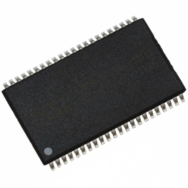
IS61WV5128ALL/ALS
IS61WV5128BLL/BLS
IS64WV5128BLL/BLS
512K x 8 HIGH-SPEED ASYNCHRONOUS CMOS STATIC RAM
AUGUST 2009
FEATURES
HIGH SPEED: (IS61/64WV5128ALL/BLL)
• High-speed access time: 8, 10, 20 ns
• Low Active Power: 85 mW (typical)
• Low stand-by power: 7 mW (typical)
CMOS standby
LOW POWER: (IS61/64WV5128ALS/BLS)
• High-speed access time: 25, 35 ns
• Low Active Power: 35 mW (typical)
• Low stand-by power: 0.6 mW (typical)
CMOS standby
• Single power supply
— Vdd 1.65V to 2.2V (IS61WV5128Axx)
— Vdd 2.4V to 3.6V (IS61/64WV5128Bxx)
• Fully static operation: no clock or refresh
required
• Three state outputs
• Industrial and Automotive temperature support
• Lead-free available
DESCRIPTION
The ISSI IS61WV5128Axx and IS61/64WV5128Bxx
are very high-speed, low power, 524,288-word by
8-bit CMOS static RAMs. The IS61WV5128Axx and
IS61/64WV5128Bxx are fabricated using ISSI's highperformance CMOS technology. This highly reliable process coupled with innovative circuit design techniques,
yields higher performance and low power consumption
devices.
When CE is HIGH (deselected), the device assumes
a standby mode at which the power dissipation can be
reduced down with CMOS input levels.
The IS61WV5128Axx and IS61/64WV5128Bxx operate
from a single power supply.
The IS61WV5128ALL and IS61/64WV5128BLL are available in 36-pin 400-mil SOJ, 36-pin mini BGA, and 44-pin
TSOP (Type II) packages.
The IS61WV5128ALS and IS61/64WV5128BLS are
available in 32-pinTSOP (Type I), 32-pin sTSOP (Type I),
32-pin SOP and 32-pin TSOP (Type II) packages.
FUNCTIONAL BLOCK DIAGRAM
A0-A18
DECODER
512K X 8
MEMORY ARRAY
I/O
DATA
CIRCUIT
COLUMN I/O
VDD
GND
I/O0-I/O7
CE
OE
CONTROL
CIRCUIT
WE
Copyright © 2006 Integrated Silicon Solution, Inc. All rights reserved. ISSI reserves the right to make changes to this specification and its products at any time without
notice. ISSI assumes no liability arising out of the application or use of any information, products or services described herein. Customers are advised to obtain the latest version of this device specification before relying on any published information and before placing orders for products.
Integrated Silicon Solution, Inc. — www.issi.com
Rev. I
08/10/09
1
�IS61WV5128ALL/ALS, IS61WV5128BLL/BLS
IS64WV5128BLL/BLS
PIN CONFIGURATION (HIGH SPEED) (61/64WV5128ALL/BLL)
44-Pin TSOP (Type II)
36 mini BGA
1
2
3
4
5
6
A
A0
A1
NC
A3
A6
A8
B
I/O4
A2
WE
A4
A7
I/O0
NC
A5
C
I/O5
D
GND
VDD
E
VDD
GND
F
I/O6
G
I/O7
H
A9
2
I/O2
A18
A17
OE
CE
A16
A15
I/O3
A10
A11
A12
A13
A14
PIN DESCRIPTIONS
A0-A18
CE
OE
WE
I/O0-I/O7
Vdd
GND
NC
I/O1
Address Inputs
Chip Enable Input
Output Enable Input
Write Enable Input
Bidirectional Ports
Power
Ground
No Connection
NC
NC
A0
A1
A2
A3
A4
CE
I/O0
I/O1
VDD
GND
I/O2
I/O3
WE
A5
A6
A7
A8
A9
NC
NC
44
43
42
41
40
39
38
37
36
35
34
33
32
31
30
29
28
27
26
25
24
23
1
2
3
4
5
6
7
8
9
10
11
12
13
14
15
16
17
18
19
20
21
22
NC
NC
NC
A18
A17
A16
A15
OE
I/O7
I/O6
GND
VDD
I/O5
I/O4
A14
A13
A12
A11
A10
NC
NC
NC
36-Pin SOJ
A0
1
36
NC
A1
2
35
A18
A2
3
34
A17
A3
4
33
A16
A4
5
32
A15
CE
6
31
OE
I/O0
7
30
I/O7
I/O1
8
29
I/O6
VDD
9
28
GND
GND
10
27
VDD
I/O2
11
26
I/O5
I/O3
12
25
I/O4
WE
13
24
A14
A5
14
23
A13
A6
15
22
A12
A7
16
21
A11
A8
17
20
A10
A9
18
19
NC
Integrated Silicon Solution, Inc. — www.issi.com
Rev. I
08/10/09
�IS61WV5128ALL/ALS, IS61WV5128BLL/BLS
IS64WV5128BLL/BLS
PIN CONFIGURATION (LOW POWER) (61/64WV5128ALS/BLS)
32-pin TSOP (TYPE I), (Package Code T)
32-pin sTSOP (TYPE I) (Package Code H)
A11
A9
A8
A13
WE
A18
A15
VDD
A17
A16
A14
A12
A7
A6
A5
A4
32
31
30
29
28
27
26
25
24
23
22
21
20
19
18
17
1
2
3
4
5
6
7
8
9
10
11
12
13
14
15
16
OE
A10
CE
I/O7
I/O6
I/O5
I/O4
I/O3
GND
I/O2
I/O1
I/O0
A0
A1
A2
A3
32-pin SOP
32-pin TSOP (TYPE II)
(Package Code T2)
A17
A16
A14
A12
A7
A6
A5
A4
A3
A2
A1
A0
I/O0
I/O1
I/O2
GND
1
2
3
4
5
6
7
8
9
10
11
12
13
14
15
16
32
31
30
29
28
27
26
25
24
23
22
21
20
19
18
17
VDD
A15
A18
WE
A13
A8
A9
A11
OE
A10
CE
I/O7
I/O6
I/O5
I/O4
I/O3
PIN DESCRIPTIONS
A0-A18
CE
OE
WE
I/O0-I/O7
Vdd
GND
Address Inputs
Chip Enable 1 Input
Output Enable Input
Write Enable Input
Input/Output
Power
Ground
Integrated Silicon Solution, Inc. — www.issi.com
Rev. I
08/10/09
3
�IS61WV5128ALL/ALS, IS61WV5128BLL/BLS
IS64WV5128BLL/BLS
DC ELECTRICAL CHARACTERISTICS (Over Operating Range)
Vdd = 3.3V + 5%
Symbol
Voh
Vol
Vih
Vil
Ili
Ilo
Parameter
Test Conditions
Output HIGH Voltage
Vdd = Min., Ioh = –4.0 mA
Output LOW Voltage
Vdd = Min., Iol = 8.0 mA
Input HIGH Voltage
Input LOW Voltage(1)
Input Leakage
GND ≤ Vin ≤ Vdd
Output Leakage
GND ≤ Vout ≤ Vdd, Outputs Disabled
Min.
2.4
—
2
–0.3
–1
–1
Max.
—
0.4
Vdd + 0.3
0.8
1
1
Unit
V
V
V
V
µA
µA
Min.
1.8
—
2.0
–0.3
–1
–1
Max.
—
0.4
Vdd + 0.3
0.8
1
1
Unit
V
V
V
V
µA
µA
Note:
1. Vil (min.) = –0.3V DC; Vil (min.) = –2.0V AC (pulse width
IS61WV5128BLS-25TLI 价格&库存
很抱歉,暂时无法提供与“IS61WV5128BLS-25TLI”相匹配的价格&库存,您可以联系我们找货
免费人工找货