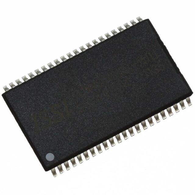
IS62C10248AL IS65C10248AL
1M x 8 LOW VOLTAGE, ULTRA LOW POWER CMOS STATIC RAM
FEATURES
• High-speed access time: 45ns, 55ns • CMOS low power operation – 36 mW (typical) operating – 12 µW (typical) CMOS standby • TTL compatible interface levels • Single power supply – 4.5V--5.5V Vdd • Three state outputs • Automotive temperature (-40oC to +125oC) • Lead-free available
PRELIMINARY INFORMATION OCTOBER 2009
speed, 8M bit static RAMs organized as 1M words by 8 bits. It is fabricated using ISSI's high-performance CMOS technology. This highly reliable process coupled with innovative circuit design techniques, yields highperformance and low power consumption devices. When CS1 is HIGH (deselected) or when CS2 is LOW (deselected), the device assumes a standby mode at which the power dissipation can be reduced down with CMOS input levels. Easy memory expansion is provided by using Chip Enable and Output Enable inputs. The active LOW Write Enable (WE) controls both writing and reading of the memory. The IS62C10248AL and IS65C10248AL are packaged in the JEDEC standard 48-pin mini BGA (9mm x 11mm) and 44-Pin TSOP (TYPE II).
DESCRIPTION The ISSI IS62C10248AL/IS65C10248AL are high-
FUNCTIONAL BLOCK DIAGRAM
A0-A19
DECODER
1M x 8 MEMORY ARRAY
VDD GND I/O DATA CIRCUIT
I/O0-I/O7
COLUMN I/O
CS2 CS1 OE WE
Copyright © 2009 Integrated Silicon Solution, Inc. All rights reserved. ISSI reserves the right to make changes to this specification and its products at any time without notice. ISSI assumes no liability arising out of the application or use of any information, products or services described herein. Customers are advised to obtain the latest version of this device specification before relying on any published information and before placing orders for products.
CONTROL CIRCUIT
Integrated Silicon Solution, Inc. — www.issi.com — 1-800-379-4774
Rev. 00A 09/25/09
1
�IS62C10248AL, IS65C10248AL
PIN CONFIGURATION (1M x 8 Low Power) 48-pin mini BGA (B) (9mm x 11mm) 44-pin TSOP (Type II)
1
A B C D E F G H
NC
2
OE
3
A0
4
A1
5
A2
6
CS2
NC
NC
A3
A4
CS1
NC
I/O0
NC
A5
A6
NC
I/O4
GND
I/O1
A17
A7
I/O5
VDD
VDD
I/O2
NC
A16
I/O6
VSS
I/O3
NC
A14
A15
NC
I/O7
NC
NC
A12
A13
WE
NC
A18
A8
A9
A10
A11
A19
A4 A3 A2 A1 A0 CS1 NC NC I/O0 I/O1 VDD GND I/O2 I/O3 NC NC WE A19 A18 A17 A16 A15
1 2 3 4 5 6 7 8 9 10 11 12 13 14 15 16 17 18 19 20 21 22
44 43 42 41 40 39 38 37 36 35 34 33 32 31 30 29 28 27 26 25 24 23
A5 A6 A7 OE CS2 A8 NC NC I/O7 I/O6 GND VDD I/O5 I/O4 NC NC A9 A10 A11 A12 A13 A14
PIN DESCRIPTIONS
A0-A19 CS1 CS2 OE WE I/O0-I/O7 NC Vdd GND Address Inputs Chip Enable 1 Input Chip Enable 2 Input Output Enable Input Write Enable Input Input/Output No Connection Power Ground
2
Integrated Silicon Solution, Inc. — www.issi.com — 1-800-379-4774
Rev. 00A 09/25/09
�IS62C10248AL, IS65C10248AL
TRUTH TABLE
Mode WE Not Selected X (Power-down) X Output Disabled H Read H Write L CS1 H X L L L CS2 X L H H H OE X X H L X I/O Operation High-Z High-Z High-Z dout din Vdd Current isb1, isb2 isb1, isb2 iCC iCC iCC
OPERATING RANGE (Vdd)
Range Ambient Temperature Vdd Speed
Commercial Industrial Automotive
0°C to +70°C –40°C to +85°C –40°C to +125°C
4.5V - 5.5V 4.5V - 5.5V 4.5V - 5.5V
45ns 55ns 55ns
CAPACITANCE(1,2)
Symbol Cin Cout Parameter Input Capacitance Output Capacitance Conditions Vin = 0V Vout = 0V Max. 5 7 Unit pF pF
Notes: 1. Tested initially and after any design or process changes that may affect these parameters. 2. Test conditions: Ta = 25°C, f = 1 MHz, Vdd = 5.0V.
Integrated Silicon Solution, Inc. — www.issi.com — 1-800-379-4774
Rev. 00A 09/25/09
3
�IS62C10248AL, IS65C10248AL
ABSOLUTE MAXIMUM RATINGS(1)
Symbol Vterm tstg Pt iout Parameter Terminal Voltage with Respect to GND Storage Temperature Power Dissipation DC Output Current (LOW) Value –0.5 to +7.0 –65 to +150 1.5 20 Unit V °C W mA
Notes: 1. Stress greater than those listed under ABSOLUTE MAXIMUM RATINGS may cause permanent damage to the device. This is a stress rating only and functional operation of the device at these or any other conditions above those indicated in the operational sections of this specification is not implied. Exposure to absolute maximum rating conditions for extended periods may affect reliability.
DC ELECTRICAL CHARACTERISTICS (Over Operating Range)
Symbol Parameter Voh Vol Vih Vil ili Output HIGH Voltage Output LOW Voltage Input HIGH Voltage Input LOW Voltage(1) Input Leakage Test Conditions Vdd = Min., ioh = –1 mA Vdd = Min., iol = 2.1 mA GND ≤ Vin ≤ Vdd Com. Ind. Auto. Com. Ind. Auto. Min. 2.4 — 2.2 –0.3 –1 –2 –5 –1 –2 –5 Max. — 0.4 Vdd + 0.5 0.8 1 2 5 1 2 5 Unit V V V V µA
ilo
Output Leakage
GND ≤ Vout ≤ Vdd Outputs Disabled
µA
Note: 1. Vil (min) = -0.3V DC; Vil (min) = -2.0V AC (pulse width -2.0 ns). Not 100% tested. Vih (max) = Vdd + 0.3V DC; Vih (max) = Vdd + 2.0V AC (pulse width -2.0 ns). Not 100% tested.
4
Integrated Silicon Solution, Inc. — www.issi.com — 1-800-379-4774
Rev. 00A 09/25/09
�IS62C10248AL, IS65C10248AL
AC TEST CONDITIONS
Parameter Input Pulse Level Input Rise and Fall Times Input and Output Timing and Reference Level Output Load Unit 0V to 3.0V 5 ns 1.5V See Figures 1 and 2
AC TEST LOADS
481 Ω 5V OUTPUT 30 pF Including jig and scope 255 Ω
5V OUTPUT 5 pF Including jig and scope 255 Ω 481 Ω
Figure 1
Figure 2
Integrated Silicon Solution, Inc. — www.issi.com — 1-800-379-4774
Rev. 00A 09/25/09
5
�IS62C10248AL, IS65C10248AL
POWER SUPPLY CHARACTERISTICS(1) (Over Operating Range)
-45 ns Symbol Parameter iCC Vdd Dynamic Operating Supply Current Test Conditions Min. Com. Ind. Auto. typ
(2)
-55 ns Min. — — Max. Unit mA 25 40 12
Max. 25
Vdd = Max., CS1 = Vil, CS2 = Vih iout = 0 mA Vin = Vih or Vil f = fmax
—
13 — 10 — — — 1 — — — 40 — — 15
iCC1
Average operating
Current
CS1 = Vil, Cs2 = Vih i i/o = 0 mA Vin = Vih or Vil Vdd = Max., CS1 ≥ Vih, CS2 ≤ Vil Vin = Vih or Vil f=0 Vdd = Max., CS1≥ Vdd – 0.2V and CS2 ≤ Vss + 0.2V Vin ≥ Vdd – 0.2V or Vin ≤ Vss + 0.2V f=0
Com. Ind. Auto. Com. Ind. Auto. Com. Ind. Auto. typ
(2)
mA 10 20 mA 1.5 2
Isb1
TTL Standby Current (TTL Inputs)
Isb2
CMOS Standby Current (CMOS Inputs)
µA
60 180
Note: 1. At f = fmax, address and data inputs are cycling at the maximum frequency, f = 0 means no input lines change. 2. Typical Values are measured at Vcc = 5V, Ta = 25oC and not 100% tested.
6
Integrated Silicon Solution, Inc. — www.issi.com — 1-800-379-4774
Rev. 00A 09/25/09
�IS62C10248AL, IS65C10248AL
READ CYCLE SWITCHING CHARACTERISTICS(1) (Over Operating Range)
Symbol trC taa toha Parameter Read Cycle Time Address Access Time Output Hold Time CS1/CS2 Access Time OE Access Time OE to High-Z Output OE to Low-Z Output CS1/CS2 to High-Z Output CS1/CS2 to Low-Z Output 45 ns Min. 45 — 10 — — — 5 0 10 55 ns Max. — 45 — 45 20 15 — 15 — Min. 55 — 10 — — — 5 0 10 Max. — 55 — 55 25 20 — 20 — Unit ns ns ns ns ns ns ns ns ns
taCs1/taCs2 tdoe thzoe(2) tlzoe(2) thzCs1/thzCs2(2) tlzCs1/tlzCs2(2)
Notes: 1. Test conditions assume signal transition times of 5 ns or less, timing reference levels of 1.5V, input pulse levels of 0V to 3.0V and output loading specified in Figure 1. 2. Tested with the load in Figure 2. Transition is measured ±500 mV from steady-state voltage. Not 100% tested.
AC WAVEFORMS READ CYCLE NO. 1(1,2) (Address Controlled) (CS1 = OE = Vil, Cs2 = WE = Vih)
tRC
ADDRESS
tAA tOHA tOHA
DATA VALID
DOUT
PREVIOUS DATA VALID
Integrated Silicon Solution, Inc. — www.issi.com — 1-800-379-4774
Rev. 00A 09/25/09
7
�IS62C10248AL, IS65C10248AL
AC WAVEFORMS READ CYCLE NO. 2(1,3) (CS1, CS2, AND OE Controlled)
tRC
ADDRESS
tAA tOHA
OE
tDOE tHZOE
CS1
tACS1/tACS2
tLZOE
CS2
tLZCS1/ tLZCS2
HIGH-Z
tHZCS
DATA VALID
DOUT
Notes: 1. WE is HIGH for a Read Cycle. 2. The device is continuously selected. OE, CS1 = Vil. Cs2=WE=Vih. 3. Address is valid prior to or coincident with CS1 LOW and CS2 HIGH transition.
8
Integrated Silicon Solution, Inc. — www.issi.com — 1-800-379-4774
Rev. 00A 09/25/09
�IS62C10248AL, IS65C10248AL
WRITE CYCLE SWITCHING CHARACTERISTICS(1,2) (Over Operating Range)
Symbol twC Parameter Write Cycle Time CS1/CS2 to Write End Address Setup Time to Write End Address Hold from Write End Address Setup Time WE Pulse Width Data Setup to Write End Data Hold from Write End WE LOW to High-Z Output WE HIGH to Low-Z Output 45ns Min. Max. 45 — 35 — 35 — 0 — 0 — 35 — 25 — 0 — — 20 5 — 55 ns Min. 55 45 45 0 0 40 30 0 — 5 Max. — — — — — — — — 20 — Unit ns ns ns ns ns ns ns n s ns ns
tsCs1/tsCs2 taw tha tsa tPwe(4) tsd thd thzwe(3) tlzwe(3)
Notes:
1. Test conditions assume signal transition times of 5 ns or less, timing reference levels of 1.5V, input pulse levels of 0V to 3.0V and output loading specified in Figure 1. 2. The internal write time is defined by the overlap of CS1 LOW, CS2 HIGH, and WE LOW. All signals must be in valid states to initiate a Write, but any one can go inactive to terminate the Write. The Data Input Setup and Hold timing are referenced to the rising or falling edge of the signal that terminates the write. 3. Tested with the load in Figure 2. Transition is measured ±500 mV from steady-state voltage. Not 100% tested. 4. tPwe > thzwe + tsd when OE is LOW.
AC WAVEFORMS WRITE CYCLE NO. 1 (CS1/CS2 Controlled, OE = HIGH or LOW)
tWC
ADDRESS
tSCS1 tHA
CS1
tSCS2
CS2
tAW tPWE tSA tHZWE
HIGH-Z
WE
tLZWE
DOUT
DATA UNDEFINED
tSD
tHD
DIN
DATA-IN VALID
Integrated Silicon Solution, Inc. — www.issi.com — 1-800-379-4774
Rev. 00A 09/25/09
9
�IS62C10248AL, IS65C10248AL
WRITE CYCLE NO. 2 (WE Controlled: OE is HIGH During Write Cycle)
tWC
ADDRESS
OE
tSCS1 tHA
CS1
tSCS2
CS2
tAW tPWE tSA tHZWE
HIGH-Z
WE
tLZWE
DOUT
DATA UNDEFINED
tSD
tHD
DIN
DATA-IN VALID
WRITE CYCLE NO. 3 (WE Controlled: OE is LOW During Write Cycle)
tWC
ADDRESS
OE
tSCS1 tHA
CS1
tSCS2
CS2
tAW tPWE tSA tHZWE
HIGH-Z
WE
tLZWE
DOUT
DATA UNDEFINED
tSD
tHD
DIN
DATA-IN VALID
10
Integrated Silicon Solution, Inc. — www.issi.com — 1-800-379-4774
Rev. 00A 09/25/09
�IS62C10248AL, IS65C10248AL
DATA RETENTION SWITCHING CHARACTERISTICS (4.5V - 5.5V)
Symbol Vdr idr Parameter Vdd for Data Retention Data Retention Current Test Condition See Data Retention Waveform Vdd = 2.0V and CS1 ≥ Vdd – 0.2V and (a) CS2 ≥ Vdd – 0.2V or (b) CS2 ≤ GND + 0.2V Data Retention Setup Time See Data Retention Waveform Recovery Time See Data Retention Waveform Com. Ind. Auto. Min. 2.0 — — — — 0 trC Typ.(1) 15 — — Max. 5.5 20 40 60 180 — — Unit V µA ns ns
tsdr trdr
Note: 1. Typical Values are measured at Vcc = 5V, Ta = 25oC and not 100% tested.
DATA RETENTION WAVEFORM (CS1 Controlled)
tSDR VDD 1.65V Data Retention Mode tRDR
1.4V
VDR CS1 ≥ VDD - 0.2V
CS1 GND
DATA RETENTION WAVEFORM (CS2 Controlled)
Data Retention Mode VDD CE2 2.2V VDR 0.4V GND CS2 ≤ 0.2V tSDR tRDR
3.0
Integrated Silicon Solution, Inc. — www.issi.com — 1-800-379-4774
Rev. 00A 09/25/09
11
�IS62C10248AL, IS65C10248AL
IS62C10248AL (4.5V - 5.5V) Industrial Range: –40°C to +85°C
Speed (ns) 55 Order Part No.* IS62C10248AL-55TLI IS62C10248AL-55MLI Package TSOP-II, Lead-free mini BGA, Lead-free (9mmx11mm)
*Devices will meet 45ns when used in 0oC to +70oC temperature range.
IS65C10248AL (4.5V - 5.5V) Industrial Range: –40°C to +125°C
Speed (ns) 55 Order Part No. IS65C10248AL-55CTLA3 IS65C10248AL-55MLA3 Package TSOP-II, Lead-free, Copper Lead-frame mini BGA, Lead-free (9mmx11mm)
12
Integrated Silicon Solution, Inc. — www.issi.com — 1-800-379-4774
Rev. 00A 09/25/09
�Rev. 00A 09/25/09
IS62C10248AL, IS65C10248AL
Integrated Silicon Solution, Inc. — www.issi.com — 1-800-379-4774
Θ
NOTE :
1. CONTROLLING DIMENSION : MM 2. DIMENSION D AND E1 DO NOT INCLUDE MOLD PROTRUSION. 3. DIMENSION b DOES NOT INCLUDE DAMBAR PROTRUSION/INTRUSION.
Θ
Package Outline
06/04/2008
13
�IS62C10248AL, IS65C10248AL
08/21/2008
14 Integrated Silicon Solution, Inc. — www.issi.com — 1-800-379-4774
Rev. 00A 09/25/09
NOTE :
1. CONTROLLING DIMENSION : MM . 2. Reference document : JEDEC MO-207
�