IS62C25616BL-45TLI-TR 数据手册
IS62C25616BL, IS65C25616BL
256K x 16 HIGH-SPEED CMOS STATIC RAM
MARCH 2013
FEATURES
• High-speed access time: 45 ns
• Low Active Power: 50 mW (typical)
• Low Standby Power: 10 mW (typical)
CMOS standby
• TTL compatible interface levels
• Single 5V ± 10% power supply
• Fully static operation: no clock or refresh
required
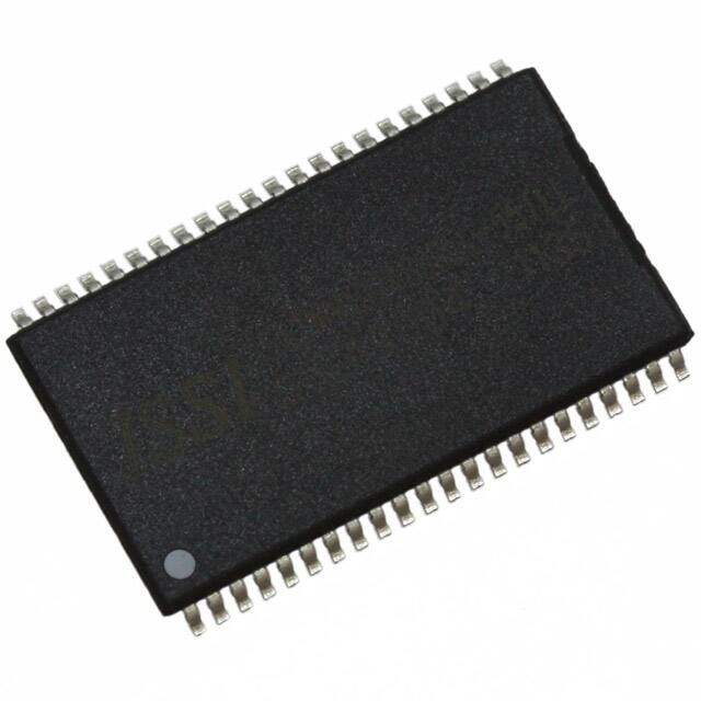
• Package: 44-pin TSOP (Type II)
• Commercial, Industrial and Automotive temperature ranges available
• Lead-free available
DESCRIPTION
The ISSI IS62C25616BL and IS65C25616BL are high-
speed, 4,194,304-bit static RAMs organized as 262,144
words by 16 bits. They are fabricated using ISSI's highperformance CMOS technology.This highly reliable process
coupled with innovative circuit design techniques, yields
access times as fast as 12 ns with low power consumption.
When CE is HIGH (deselected), the device assumes a
standby mode at which the power dissipation can be reduced
down with CMOS input levels.
Easy memory expansion is provided by using Chip Enable
and Output Enable inputs, CE and OE. The active LOW
Write Enable (WE) controls both writing and reading of the
memory. A data byte allows Upper Byte (UB) and Lower
Byte (LB) access.
The IS62C25616BL and IS65C25616BL are packaged in
the JEDEC standard 44-pin TSOP (Type II).
FUNCTIONAL BLOCK DIAGRAM
A0-A17
DECODER
256K x 16
MEMORY ARRAY
I/O
DATA
CIRCUIT
COLUMN I/O
VDD
GND
I/O0-I/O7
Lower Byte
I/O8-I/O15
Upper Byte
CE
OE
WE
UB
LB
CONTROL
CIRCUIT
Copyright © 2013 Integrated Silicon Solution, Inc. All rights reserved. ISSI reserves the right to make changes to this specification and its products at any time without
notice. ISSI assumes no liability arising out of the application or use of any information, products or services described herein. Customers are advised to obtain the latest version of this device specification before relying on any published information and before placing orders for products.
Integrated Silicon Solution, Inc. does not recommend the use of any of its products in life support applications where the failure or malfunction of the product can reasonably be expected to cause failure of the life support system or to significantly affect its safety or effectiveness. Products are not authorized for use in such applications
unless Integrated Silicon Solution, Inc. receives written assurance to its satisfaction, that:
a.) the risk of injury or damage has been minimized;
b.) the user assume all such risks; and
c.) potential liability of Integrated Silicon Solution, Inc is adequately protected under the circumstances
Integrated Silicon Solution, Inc. — www.issi.com — 1-800-379-4774
Rev. B
03/15/2013
1
�IS62C25616BL, IS65C25616BL
PIN CONFIGURATIONS*
44-Pin TSOP (Type II)
A4
A3
A2
A1
A0
CE
I/O0
I/O1
I/O2
I/O3
VDD
GND
I/O4
I/O5
I/O6
I/O7
WE
A16
A15
A14
A13
A12
44
43
42
41
40
39
38
37
36
35
34
33
32
31
30
29
28
27
26
25
24
23
1
2
3
4
5
6
7
8
9
10
11
12
13
14
15
16
17
18
19
20
21
22
A5
A6
A7
OE
UB
LB
I/O15
I/O14
I/O13
I/O12
GND
VDD
I/O11
I/O10
I/O9
I/O8
NC
A8
A9
A10
A11
A17
*Please contact ISSI at SRAM@issi.com for availability of 48-pin BGA and 44-pin SOJ packages.
PIN DESCRIPTIONS
A0-A17
I/O0-I/O15
CE
OE
WE
Address Inputs
Data Inputs/Outputs
Chip Enable Input
Output Enable Input
Write Enable Input
LB
UB
NC
Vdd
GND
Lower-byte Control (I/O0-I/O7)
Upper-byte Control (I/O8-I/O15)
No Connection
Power
Ground
2 Integrated Silicon Solution, Inc. — www.issi.com — 1-800-379-4774
Rev. B
03/15/2013
�IS62C25616BL, IS65C25616BL
TRUTH TABLE
I/O PIN
Mode
WE
CE
OE
LB
UB
I/O0-I/O7 I/O8-I/O15
Not Selected
X
H
X
X
X
High-Z
High-Z
Output Disabled
H
L
H
X
X
High-Z
High-Z
X
L
X
H
H
High-Z
High-Z
Read
H
L
L
L
H
Dout
High-Z
H
L
L
H
L
High-Z
Dout
H
L
L
L
L Dout Dout
Write
L
L
X
L
H
Din
High-Z
L
L
X
H
L
High-Z
Din
L
L
X
L
L Din Din
Vdd Current
Isb1, Isb2
Icc1, Icc2
Icc1, Icc2
Icc1, Icc2
ABSOLUTE MAXIMUM RATINGS(1)
Symbol
Vterm
Tstg
Pt
Iout
Parameter
Terminal Voltage with Respect to GND
Storage Temperature
Power Dissipation
DC Output Current (LOW)
Value
–0.5 to +7.0
–65 to +150
1.5
20
Unit
V
°C
W
mA
Notes:
1. Stress greater than those listed under ABSOLUTE MAXIMUM RATINGS may cause permanent damage to the
device. This is a stress rating only and functional operation of the device at these or any other conditions above
those indicated in the operational sections of this specification is not implied. Exposure to absolute maximum rating
conditions for extended periods may affect reliability.
CAPACITANCE(1,2)
Symbol
Cin
Cout
Parameter
Input Capacitance
Output Capacitance
Conditions
Vin = 0V
Vout = 0V
Max.
6
8
Unit
pF
pF
Notes:
1. Tested initially and after any design or process changes that may affect these parameters.
2. Test conditions: Ta = 25°C, f = 1 MHz, Vdd = 5.0V.
DC ELECTRICAL CHARACTERISTICS (Over Operating Range)
Symbol
Voh
Vol
Vih
Vil
Ili
Ilo
Parameter
Output HIGH Voltage
Output LOW Voltage
Input HIGH Voltage(1)
Input LOW Voltage(1)
Input Leakage
Output Leakage
Test Conditions
Vdd = Min., Ioh = –1.0 mA
Vdd = Min., Iol = 2.1 mA
GND ≤ Vin ≤ Vdd
Com.
Ind.
Auto.
GND ≤ Vout ≤ Vdd
Com.
Outputs Disabled
Ind.
Auto.
Min.
2.4
—
2.2
–0.3
–1
–2
–5
–1
–2
–5
Max.
—
0.4
Vdd + 0.5
0.8
1
2
5
1
2
5
Unit
V
V
V
V
µA
µA
Note:
1. Vill (min) = -2.0V AC (pulse width
IS62C25616BL-45TLI-TR 价格&库存
很抱歉,暂时无法提供与“IS62C25616BL-45TLI-TR”相匹配的价格&库存,您可以联系我们找货
免费人工找货