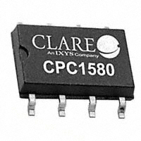
CPC1580
Optically Isolated
Gate Drive Circuit
INTEGRATED CIRCUITS DIVISION
Features
•
•
•
•
•
•
•
•
Description
Drives External Power MOSFET
Low LED Current (2.5mA)
Requires No External Power Supply
Load Voltages up to 65V
High Reliability
Small 8-pin Surface Mount Package
3750Vrms Input/Output Isolation
Flammability Rating UL 94 V-0
The CPC1580 optical gate driver provides isolated
control of a discrete power MOSFET transistor without
the need of an external power supply. Control of the
power MOSFET transistor is accomplished by the
application of sufficient input LED current to activate
the driver circuitry.
On the load side, an external storage capacitor and an
internal bootstrap diode enable the internal
photovoltaic and gate driver circuitry to provide fast
output switching characteristics by supplying the
charge necessary to satisfy the MOSFET’s bias
requirements.
Applications
•
•
•
•
•
•
Industrial Controls
Instrumentation
Medical Equipment Isolation
Electronic Switching
I/O Subsystems
Appliances
Provided in a small 8-pin package, the CPC1580
provides 3750Vrms of input-to-output isolation.
Ordering Information
Approvals
• UL recognized component: File # E76270
Part
Description
CPC1580P
8-Pin Flatpack (50/Tube)
CPC1580PTR
8-Pin Flatpack (1000/Reel)
Figure 1. CPC1580 DC Application Circuit Diagram
CPC1580
1
4
NC
CST
8 VCAP
7
LOAD
VD
NC
+VLOAD
5
LED +
LED -
2
3
VG
6
VS
DS-CPC1580-R02
www.ixysic.com
Q1
-VLOAD
1
�INTEGRATED CIRCUITS DIVISION
CPC1580
1. Specifications . . . . . . . . . . . . . . . . . . . . . . . . . . . . . . . . . . . . . . . . . . . . . . . . . . . . . . . . . . . . . . . . . . . . . . . . . . . . . . . . . . . . . . . . . . . . . .
1.1 Package Pinout . . . . . . . . . . . . . . . . . . . . . . . . . . . . . . . . . . . . . . . . . . . . . . . . . . . . . . . . . . . . . . . . . . . . . . . . . . . . . . . . . . . . . . . . .
1.2 Pin Description. . . . . . . . . . . . . . . . . . . . . . . . . . . . . . . . . . . . . . . . . . . . . . . . . . . . . . . . . . . . . . . . . . . . . . . . . . . . . . . . . . . . . . . . . .
1.3 Absolute Maximum Ratings . . . . . . . . . . . . . . . . . . . . . . . . . . . . . . . . . . . . . . . . . . . . . . . . . . . . . . . . . . . . . . . . . . . . . . . . . . . . . . . .
1.4 ESD Rating . . . . . . . . . . . . . . . . . . . . . . . . . . . . . . . . . . . . . . . . . . . . . . . . . . . . . . . . . . . . . . . . . . . . . . . . . . . . . . . . . . . . . . . . . . . .
1.5 Recommended Operating Conditions . . . . . . . . . . . . . . . . . . . . . . . . . . . . . . . . . . . . . . . . . . . . . . . . . . . . . . . . . . . . . . . . . . . . . . . .
1.6 General Conditions . . . . . . . . . . . . . . . . . . . . . . . . . . . . . . . . . . . . . . . . . . . . . . . . . . . . . . . . . . . . . . . . . . . . . . . . . . . . . . . . . . . . . .
1.7 Electrical Specifications . . . . . . . . . . . . . . . . . . . . . . . . . . . . . . . . . . . . . . . . . . . . . . . . . . . . . . . . . . . . . . . . . . . . . . . . . . . . . . . . . . .
1.8 Performance Data* . . . . . . . . . . . . . . . . . . . . . . . . . . . . . . . . . . . . . . . . . . . . . . . . . . . . . . . . . . . . . . . . . . . . . . . . . . . . . . . . . . . . . .
3
3
3
3
3
3
4
4
5
2. Introduction . . . . . . . . . . . . . . . . . . . . . . . . . . . . . . . . . . . . . . . . . . . . . . . . . . . . . . . . . . . . . . . . . . . . . . . . . . . . . . . . . . . . . . . . . . . . . . . . 6
3. Functional Description . . . . . . . . . . . . . . . . . . . . . . . . . . . . . . . . . . . . . . . . . . . . . . . . . . . . . . . . . . . . . . . . . . . . . . . . . . . . . . . . . . . . . . . 6
4. Device Configuration. . . . . . . . . . . . . . . . . . . . . . . . . . . . . . . . . . . . . . . . . . . . . . . . . . . . . . . . . . . . . . . . . . . . . . . . . . . . . . . . . . . . . . . . .
4.1 LED Resistor . . . . . . . . . . . . . . . . . . . . . . . . . . . . . . . . . . . . . . . . . . . . . . . . . . . . . . . . . . . . . . . . . . . . . . . . . . . . . . . . . . . . . . . . . . .
4.2 Storage Capacitor Selection . . . . . . . . . . . . . . . . . . . . . . . . . . . . . . . . . . . . . . . . . . . . . . . . . . . . . . . . . . . . . . . . . . . . . . . . . . . . . . .
4.3 Transistor Selection . . . . . . . . . . . . . . . . . . . . . . . . . . . . . . . . . . . . . . . . . . . . . . . . . . . . . . . . . . . . . . . . . . . . . . . . . . . . . . . . . . . . . .
4.3.1 Transistor Switching Characteristics. . . . . . . . . . . . . . . . . . . . . . . . . . . . . . . . . . . . . . . . . . . . . . . . . . . . . . . . . . . . . . . . . . . .
6
6
6
7
7
5. CPC1580 Over-Voltage Protection . . . . . . . . . . . . . . . . . . . . . . . . . . . . . . . . . . . . . . . . . . . . . . . . . . . . . . . . . . . . . . . . . . . . . . . . . . . . . . 8
5.1 Other Protection Techniques . . . . . . . . . . . . . . . . . . . . . . . . . . . . . . . . . . . . . . . . . . . . . . . . . . . . . . . . . . . . . . . . . . . . . . . . . . . . . . . 9
6. Application Switching Losses . . . . . . . . . . . . . . . . . . . . . . . . . . . . . . . . . . . . . . . . . . . . . . . . . . . . . . . . . . . . . . . . . . . . . . . . . . . . . . . . . 9
6.1 Resistive Load Losses: The Ideal Case. . . . . . . . . . . . . . . . . . . . . . . . . . . . . . . . . . . . . . . . . . . . . . . . . . . . . . . . . . . . . . . . . . . . . . 10
6.2 Inductive/Resistive Loads . . . . . . . . . . . . . . . . . . . . . . . . . . . . . . . . . . . . . . . . . . . . . . . . . . . . . . . . . . . . . . . . . . . . . . . . . . . . . . . . 10
6.3 Capacitive Loads . . . . . . . . . . . . . . . . . . . . . . . . . . . . . . . . . . . . . . . . . . . . . . . . . . . . . . . . . . . . . . . . . . . . . . . . . . . . . . . . . . . . . . . 10
6.4 dV/dt Characteristics . . . . . . . . . . . . . . . . . . . . . . . . . . . . . . . . . . . . . . . . . . . . . . . . . . . . . . . . . . . . . . . . . . . . . . . . . . . . . . . . . . . . 10
7. Design Switching Frequency . . . . . . . . . . . . . . . . . . . . . . . . . . . . . . . . . . . . . . . . . . . . . . . . . . . . . . . . . . . . . . . . . . . . . . . . . . . . . . . . . 10
8. Manufacturing Information . . . . . . . . . . . . . . . . . . . . . . . . . . . . . . . . . . . . . . . . . . . . . . . . . . . . . . . . . . . . . . . . . . . . . . . . . . . . . . . . . . .
8.1 Moisture Sensitivity . . . . . . . . . . . . . . . . . . . . . . . . . . . . . . . . . . . . . . . . . . . . . . . . . . . . . . . . . . . . . . . . . . . . . . . . . . . . . . . . . . . . .
8.2 ESD Sensitivity . . . . . . . . . . . . . . . . . . . . . . . . . . . . . . . . . . . . . . . . . . . . . . . . . . . . . . . . . . . . . . . . . . . . . . . . . . . . . . . . . . . . . . . .
8.3 Soldering Profile. . . . . . . . . . . . . . . . . . . . . . . . . . . . . . . . . . . . . . . . . . . . . . . . . . . . . . . . . . . . . . . . . . . . . . . . . . . . . . . . . . . . . . . .
8.4 Board Wash . . . . . . . . . . . . . . . . . . . . . . . . . . . . . . . . . . . . . . . . . . . . . . . . . . . . . . . . . . . . . . . . . . . . . . . . . . . . . . . . . . . . . . . . . . .
8.5 CPC1580P Package . . . . . . . . . . . . . . . . . . . . . . . . . . . . . . . . . . . . . . . . . . . . . . . . . . . . . . . . . . . . . . . . . . . . . . . . . . . . . . . . . . . .
8.6 CPC1580PTR Tape and Reel Specification . . . . . . . . . . . . . . . . . . . . . . . . . . . . . . . . . . . . . . . . . . . . . . . . . . . . . . . . . . . . . . . . . .
2
www.ixysic.com
12
12
12
12
12
13
13
R02
�INTEGRATED CIRCUITS DIVISION
CPC1580
1. Specifications
1.1 Package Pinout
1.3 Absolute Maximum Ratings
CPC1580P Pinout
N/C
1
8
2
N/C
Parameter
VCAP
7
LED +
LED -
Absolute maximum electrical ratings are at 25°C.
3
6
4
5
Blocking Voltage (VDS)
65
VP
Reverse Input Voltage
5
V
VL2
Input Control Current
50
mA
1
A
150
mW
500
mW
3750
Vrms
Operational Temperature
-40 to +110
°C
Storage Temperature
-40 to +125
°C
Peak (10ms)
VG
Input Power Dissipation 1
2
Isolation Voltage (Input to Output)
1.2 Pin Description
Name
1
N/C
Units
VL1
Output Power Dissipation
Pin#
Rating
Description
Not connected
2
LED +
Positive input to LED
3
LED -
Negative input to LED
4
N/C
Not connected
5
VG
Output, MOSFET Gate Control
6
VL2
-Load Voltage DC, ± Load Voltage AC
7
VL1
+Load Voltage DC, ± Load Voltage AC
8
VCAP
Storage Capacitor
1
Derate linearly 1.33mW/°C
2
Derate linearly 6.0mW/°C
Absolute maximum ratings are stress ratings. Stresses in
excess of these ratings can cause permanent damage to
the device. Functional operation of the device at conditions
beyond those indicated in the operational sections of this
data sheet is not implied.
1.4 ESD Rating
ESD Rating (Human Body Model)
1000 V
1.5 Recommended Operating Conditions
Parameter
Symbol
Min
Max
Units
Load Voltage
VL
15
65
V
Input Control Current
IF
2.5
10
mA
Forward Voltage Drop
VF
1
1.5
V
Operating Temperature
TA
-40
+110
°C
R02
www.ixysic.com
3
�INTEGRATED CIRCUITS DIVISION
CPC1580
1.6 General Conditions
Unless otherwise specified, minimum and maximum values are guaranteed by production testing. Typical values are
characteristic of the device at 25°C, and are the result of engineering evaluations. They are provided for informational
purposes only, and are not part of the manufacturing testing requirements. Unless otherwise noted, all electrical
specifications are listed for TA=25°C.
1.7 Electrical Specifications
Parameter
Conditions
Symbol
Min
Typ
Max
Units
Load Side Characteristics
Gate Voltage
IF=2.5mA
8.2
IF=5mA
IF=10mA
7.5
VGS
8.7
12
9.1
V
IF=2.5mA
-40°C20M over the temperature
rating of the part.
4.3 Transistor Selection
The CPC1580 charges and discharges an external
MOSFET transistor. The selection of the MOSFET is
determined by the user to meet the specific power
requirements for the load. The CPC1580 output
voltage is listed in the specifications, but as mentioned
earlier, there must be little or no gate leakage.
Another parameter that plays a significant role in the
selection of the transistor is the gate drive voltage
available from the part. The CPC1580 uses
photovoltaic cells to collect the optical energy
generated by the LED; to generate more voltage, the
photovoltaic diodes are stacked. The voltage change
of the photovoltaic stack reduces with increased
temperature. The user must select a transistor that will
maintain the load current at the maximum
temperature, given the VGS in Section 1.7, the
CPC1580 Table of Electrical Specifications.
The example circuits shown in Figure 1 and Figure 3
use “logic level” MOSFETs for each design to maintain
the load described.
4.3.1 Transistor Switching Characteristics
The primary characteristics of the application
switching are ton, toff, tRISE, tFALL, and the recovery
time of the storage capacitor, tCHG. These parameters
are dependent on the MOSFET selection and need to
be reviewed in light of the application requirements.
The CPC1580 turns on the MOSFET transistor to the
specified VGS after the ton delay. Similarly the toff delay
is the amount of time until the LED is turned off and
the capacitive load discharges to the level in the
CPC1580 specification. For MOSFETs with larger or
smaller required gate charge the ton and toff will be
proportionately faster and slower, but it is not a linear
relationship.
To calculate the nominal rise time of the transistor's
drain voltage, VD:
tRISE,VD
~
(SECONDS)
IG_SINK
To calculate the nominal fall time of the transistor's
drain voltage, VD:
tFALL,VD ~
R02
VLOAD • CRSS
www.ixysic.com
VLOAD • CRSS
IG_SOURCE
(SECONDS)
7
�INTEGRATED CIRCUITS DIVISION
CPC1580
Where CRSS is the MOSFET gate-drain capacitance
(averaged over the switching voltage range) found in
the MOSFET data sheet, IG_SINK is the gate sinking
current of the CPC1580, and IG_SOURCE is the gate
driving ability. The maximum value of tRISE is limited
by the CPC1580 unloaded discharge characteristic
and should be reviewed in light of the final application
component selections if critical.
ROVP and COVP are optional over-voltage protection
elements that are present in the application circuit
diagram (see Figure 3).
The term inside the logarithm reflects the discharge
and recharge voltage on CST. For practical circuit
component selection, this can be simplified as
described above.
Use this information to calculate the maximum
switching frequency in Section 7 below.
The value for the charge time, tCHG, is due to external
component selection. The storage capacitor charge
recovery time (seconds) is computed as:
tCHG
~ - (400 + ROVP) • (CST + COVP) • ln
(
(VLOAD - VFINAL) • CST
QG
Note: The CPC1580 is ideal to use where
remote power is otherwise unavailable. If the
LED is also powered remotely, care must be
taken to ensure that parasitic transient signals
are reliably filtered from the input control signal.
Large transient currents will mutually couple
energy between cables and a simple R-C
filtering of the CPC1580 input may be sufficient
to suppress false turn-on.
)
Which reduces to:
tCHG
~ - (400 + ROVP) • (CST + COVP) • 3
Figure 2. CPC1580 AC Application Circuit
CPC1580
1
4
*
8 VCAP
NC
CST
7
LED -
2
+/- VLOAD
Q1
5
LED +
LOAD
VD
NC
VG
Q2
3
6
+/- VLOAD
VS
* Minimum Blocking Voltage = 100V
5. CPC1580 Over-Voltage Protection
Over-voltage protection is generally required for the
CPC1580 because of parasitic inductance in the load,
wires, board traces, and axial leads of protectors.
Purely resistive loads or loads with low voltage
switching may be able to rely on the transistor to
handle any parasitic energy and thereby not require
8
protection for the CPC1580. For very low inductance
loads and traces, over-voltage suppression may be
handled with a simple R-C filter consisting of ROVP
and COVP, or by use of a free-wheeling diode (see
Figure 3). For more moderate load inductance, or
remote switching of a load (i.e. through a long cable) a
voltage suppressor can be used. For heavily inductive
loads only a free-wheeling diode, DOVP, connected
www.ixysic.com
R02
�INTEGRATED CIRCUITS DIVISION
CPC1580
across the load element is recommended, see
Figure 3.
The consequence of increasing the gate-drain
effective capacitance is reduced dV/dt tolerance.
The energy not consumed in switching losses must be
absorbed by the over-voltage protection element. Most
protective devices are designed to withstand certain
peak power, in the case of a Transient Voltage
Suppressor (TVS); or maximum avalanche energy, in
the case of a MOSFET. Understanding the switching
losses and load dynamics is absolutely essential.
When used in a circuit with an inductive load,
precautions must be taken to prevent damage to the
circuit from inductively generated voltage spikes. The
circuit shown in Figure 3 includes such protection
across the inductive load.
5.1 Other Protection Techniques
One simple way to reduce the amount of stored
inductive energy is to increase the energy dissipated
in the switch. This can be accomplished by adding a
larger capacitor in parallel with the gate-drain
connection of the MOSFET, however care must be
taken so that the rise time and peak current do not
exceed the Safe Operating Area (SOA) rating of the
transistor.
Switching loads with higher inductance characteristics
requires consideration of other circuit protection
techniques, device ratings, or protector types. Of
paramount importance is that the designer know the
characteristics of the load being switched.
Figure 3. CPC1580 Over-Voltage Protection for Inductive Loads
DOVP
CPC1580
1
4
CST
8 VCAP
NC
ROVP
7
VD
NC
ZLOAD
+VLOAD
COVP
RLED
VIN+
VIN-
5
2
VG
LED +
3
LED -
Q1
6
-VLOAD
VS
6. Application Switching Losses
During the transition intervals, the application and load
components change energy states and, in the
process, incur switching losses. The switching losses
are manifested as heat in the application circuit and
must be addressed by the designer to ensure that no
one component exceeds its power rating. The
designer must understand the details of the load
behavior in order to adequately size and protect the
application circuit. There are three general cases to
observe: (1) purely resistive loads,
R02
(2) inductive/resistive loads, and (3) loads with
significant capacitance. Inductors and capacitors are
energy storage elements that require special
consideration for switching.
During the switching periods, energy is conserved.
Inductors turning off transfer their stored energy to
MOSFET switching losses, to the capacitance of the
load and application circuit, and to the protector.
During the turn-on interval, the inductor energy is zero,
and so the capacitive energy in the load and parasitic
elements of the switching application must be
www.ixysic.com
9
�INTEGRATED CIRCUITS DIVISION
CPC1580
dissipated by the MOSFET, in order for the load to
change state.
6.3 Capacitive Loads
The energy absorbed by the MOSFET for loads that
are more capacitive in nature occurs during the
MOSFET turn-on as opposed to the turn-off. The
energy absorbed by the MOSFET will be a function of
the load, the TVS (or other protector), and the
MOSFET drain capacitance. The MOSFET energy,
EFALL, in Joules is:
To calculate the stored inductive energy in Joules:
EL =
1
• L • ILOAD2
2
6.1 Resistive Load Losses: The Ideal Case
For purely resistive loads, the energy dissipated by
changing states occurs primarily in the MOSFET.
EFALL =
The equation describing MOSFET energy dissipation
during rise time, in Joules, is:
ERISE > VLOAD2 •
CRSS
•
IG_SINK
ILOAD
6
=
PLOAD
6
• tRISE
The average power of the MOSFET for any load type
in Watts is:
PAVG = ILOAD2 • RDSAT • D + fSWITCH • (ERISE + EFALL)
Where fSWITCH is the application switching frequency;
RDSAT is the MOSFET’s on-resistance; D is the
switch's operational duty cycle: D = ton/(ton+toff); and
EFALL is MOSFET energy dissipation during fall time,
in Joules.
6.2 Inductive/Resistive Loads
If the load is resistive and inductive, and the
inductance doesn't saturate, the load current during
turn off, tRISE, in Amps is:
ILOAD(t) =
VLOAD
RLOAD
-
IG_SINK
LLOAD • CRSS
•
( )
2
LLOAD
RLOAD
•
[
-R LOAD
RLOAD
LLOAD
LLOAD
• t
• t-1+e
]
and the MOSFET drain voltage during turn off, tRISE,
in Volts is:
VDRAIN(t) =
IG_SINK
CRSS
• t
The instantaneous power in the MOSFET will be the
product of the two equations and the energy will be the
integral of the power over time.
1
2
• (CTVS + COSS + CLOAD) • VLOAD2
COSS is the MOSFET output capacitance found in the
data sheet. As mentioned earlier, the MOSFET
switching losses occur at different times, either rising
or falling, so loads with a combination of inductance
and capacitance can also be calculated by the energy
equations described above.
6.4 dV/dt Characteristics
The application circuit shown in Figure 1 dissipates
significant energy caused by large dV/dt events. Fault
voltages across the MOSFET will turn it on for the
same reason the part turns off slowly. For dV/dt events
> IG_SINK/CRSS (from Equation 2) the application
circuit will dissipate energy proportional to the CRSS
and gFS (forward conductance) of the selected
transistor. CRSS is a function of the transistor's
on-resistance and current/power capability, so higher
load designs are more sensitive.
The CPC1580 provides an internal clamp to protect
the gate of the MOSFET from damage in such an
event. The part can withstand 100mA for short
periods, like dV/dt transients.
7. Design Switching Frequency
The maximum switching frequency is the last design
value to be calculated, because the over-voltage
protection and the storage capacitor play a significant
role in determining the result. Inasmuch as those
factors are already determined, the following gives a
good approximation for the maximum switching
frequency. The maximum switching frequency is a
function of the gate charge of the MOSFET, the
storage capacitor (CST), and ROVP. The maximum
switching frequency relationship in Hz is:
Where:
10
www.ixysic.com
R02
�INTEGRATED CIRCUITS DIVISION
fMAX <
CPC1580
1
-1
• (ton + toff + (tRISE,VD | tCHG) + tFALL,VD)
M
• M=3 (multiplication factor for temperature and process variations
• ton and toff are CPC1580 data sheet parameters
• tRISE, VD is the rise time of the drain voltage and tCHG
is the charge time of the storage capacitor and the
over-voltage protection circuitry as derived in
Section 4.3: choose the greater of tRISE,VD or tCHG
for the calculation
• tFALL,VD is the fall time across the transistor
There is no minimum switching frequency since the
CPC1580 uses photovoltaic diodes to keep the output
charged while LED current flows.
R02
www.ixysic.com
11
�INTEGRATED CIRCUITS DIVISION
CPC1580
8. Manufacturing Information
8.1 Moisture Sensitivity
All plastic encapsulated semiconductor packages are susceptible to moisture ingression. IXYS Integrated
Circuits classifies its plastic encapsulated devices for moisture sensitivity according to the latest version of
the joint industry standard, IPC/JEDEC J-STD-020, in force at the time of product evaluation. We test all of
our products to the maximum conditions set forth in the standard, and guarantee proper operation of our
devices when handled according to the limitations and information in that standard as well as to any limitations set
forth in the information or standards referenced below.
Failure to adhere to the warnings or limitations as established by the listed specifications could result in reduced
product performance, reduction of operable life, and/or reduction of overall reliability.
This product carries a Moisture Sensitivity Level (MSL) classification as shown below, and should be handled
according to the requirements of the latest version of the joint industry standard IPC/JEDEC J-STD-033.
Device
Moisture Sensitivity Level (MSL) Classification
CPC1580
MSL 1
8.2 ESD Sensitivity
This product is ESD Sensitive, and should be handled according to the industry standard JESD-625.
8.3 Soldering Profile
Provided in the table below is the Classification Temperature (TC) of this product and the maximum dwell time the
body temperature of this device may be (TC - 5)ºC or greater. The classification temperature sets the Maximum Body
Temperature allowed for this device during lead-free reflow processes. For through-hole devices, and any other
processes, the guidelines of J-STD-020 must be observed.
Device
Classification Temperature (TC)
Dwell Time (tp)
Max Reflow Cycles
CPC1580
260°C
30 seconds
3
8.4 Board Wash
IXYS Integrated Circuits recommends the use of no-clean flux formulations. Board washing to reduce or remove flux
residue following the solder reflow process is acceptable provided proper precautions are taken to prevent damage to
the device. These precautions include but are not limited to: using a low pressure wash and providing a follow up bake
cycle sufficient to remove any moisture trapped within the device due to the washing process. Due to the variability of
the wash parameters used to clean the board, determination of the bake temperature and duration necessary to
remove the moisture trapped within the package is the responsibility of the user (assembler). Cleaning or drying
methods that employ ultrasonic energy may damage the device and should not be used. Additionally, the device must
not be exposed to flux or solvents that are Chlorine- or Fluorine-based.
12
www.ixysic.com
R02
�INTEGRATED CIRCUITS DIVISION
CPC1580
8.5 CPC1580P Package
0 MIN / 0.102 MAX
(0 MIN / 0.004 MAX)
2.540 ± 0.127
(0.100 ± 0.005)
6.350 ± 0.127
(0.250 ± 0.005)
7.620 ± 0.254
(0.300 ± 0.010)
9.398 ± 0.127
(0.370 ± 0.005)
Pin 1
2.286 MAX.
(0.090 MAX.)
PCB Land Pattern
2.54
(0.10)
0.635 ± 0.127
(0.025 ± 0.005)
0.203 ± 0.013
(0.008 ± 0.0005)
9.652 ± 0.381
(0.380 ± 0.015)
8.70
(0.3425)
1.55
(0.0610)
0.65
(0.0255)
2.159 ± 0.025
(0.085 ± 0.001)
0.457 ± 0.076
(0.018 ± 0.003)
0.864 ± 0.120
(0.034 ± 0.004)
Dimensions
mm
(inches)
8.6 CPC1580PTR Tape and Reel Specification
2.00
(0.079)
330.2 DIA.
(13.00 DIA.)
Top Cover
Tape Thickness
0.102 MAX.
(0.004 MAX.)
Embossment
W = 16.00
(0.63)
7.50
(0.295)
Bo = 10.30
(0.406)
K0 = 2.70
(0.106)
K1 = 2.00
(0.079)
Embossed Carrier
4.00
(0.157)
P1 = 12.00
(0.472)
User Direction of Feed
Ao = 10.30
(0.406)
Dimensions
mm
(inches)
NOTES:
1. All dimensions carry tolerances of EIA Standard 481-2
2. The tape complies with all “Notes” for constant dimensions listed on page 5 of EIA-481-2
For additional information please visit our website at: www.ixysic.com
IXYS Integrated Circuits makes no representations or warranties with respect to the accuracy or completeness of the contents of this publication and reserves the right to make changes to
specifications and product descriptions at any time without notice. Neither circuit patent licenses nor indemnity are expressed or implied. Except as set forth in IXYS Integrated Circuits’
Standard Terms and Conditions of Sale, IXYS Integrated Circuits assumes no liability whatsoever, and disclaims any express or implied warranty, relating to its products including, but not
limited to, the implied warranty of merchantability, fitness for a particular purpose, or infringement of any intellectual property right.
The products described in this document are not designed, intended, authorized or warranted for use as components in systems intended for surgical implant into the body, or in other
applications intended to support or sustain life, or where malfunction of IXYS Integrated Circuits’ product may result in direct physical harm, injury, or death to a person or severe property or
environmental damage. IXYS Integrated Circuits reserves the right to discontinue or make changes to its products at any time without notice.
Specification: DS-CPC1580-R02
©Copyright 2018, IXYS Integrated Circuits
All rights reserved. Printed in USA.
6/18/2018
R02
www.ixysic.com
13
�