IXFC52N30P
PolarTM Power MOSFET
HiPerFETTM
VDSS
ID25
RDS(on)
trr
(Electrically Isolated Back Surface)
=
=
300V
24A
80m
200ns
N-Channel Enhancement Mode
Avalanche Rated
ISOPLUS220TM
E153432
Symbol
Test Conditions
Maximum Ratings
VDSS
TJ = 25C to 150C
300
V
VDGR
TJ = 25C to 150C, RGS = 1M
300
V
VGSS
Continuous
20
V
VGSM
Transient
30
V
ID25
TC = 25C
24
A
IDM
TC = 25C, Pulse Width Limited by TJM
150
A
IA
TC = 25C
52
A
EAS
TC = 25C
1
J
dv/dt
IS IDM, VDD VDSS, TJ 150C
10
V/ns
PD
TC = 25C
100
W
-55 ... +150
150
-55 ... +150
C
C
C
300
260
°C
°C
2500
3000
V~
V~
11..66 / 2.5..14.6
N/lb.
2
g
TJ
TJM
Tstg
TL
TSOLD
Maximum Lead Temperature for Soldering
Plastic Body for 10s
VISOL
50/60 Hz, RMS
IISOL 1mA
Md
t = 1min
t = 1s
Mounting force
Weight
G
D
S
G = Gate
S = Source
Isolated Tab
D = Drain
Features
UL Recognized Package
Silicon Chip on Direct-Copper-Bond
Substrate
- High Power Dissipation
- Isolated Mounting Surface
- 2500V~ Electrical Isolation
Fast Intrinsic Rectifier
Avalanche Rated
Low RDS(ON) and QG
Low Package Inductance
Advantages
Symbol
Test Conditions
(TJ = 25C, Unless Otherwise Specified)
Characteristic Values
Min. Typ. Max.
BVDSS
VGS = 0V, ID = 250μA
300
VGS(th)
VDS = VGS, ID = 4mA
2.5
IGSS
VGS = 20V, VDS = 0V
100 nA
IDSS
VDS = VDSS, VGS = 0V
25 A
1 mA
RDS(on)
V
5.0
Applications
V
TJ = 125C
VGS = 10V, ID = 26A, Note 1
© 2013 IXYS CORPORATION, All Rights Reserved
80 m
High Power Density
Easy to Mount
Space Savings
Switch-Mode and Resonant-Mode
Power Supplies
DC-DC Converters
Laser Drivers
AC and DC Motor Drives
Robotics and Servo Controls
DS99246G(10/13)
�IXFC52N30P
Symbol
Test Conditions
(TJ = 25C, Unless Otherwise Specified)
gfs
Characteristic Values
Min.
Typ.
Max.
VDS = 10V, ID = 26A, Note 1
20
Ciss
Coss
30
S
3490
pF
VGS = 0V, VDS = 25V, f = 1MHz
Crss
td(on)
tr
td(off)
tf
Resistive Switching Times
VGS = 10V, VDS = 0.5 • VDSS, ID = 52A
RG = 4 (External)
Qg(on)
Qgs
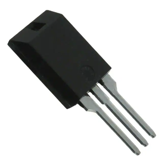
ISOPLUS220TM Outline
VGS = 10V, VDS = 0.5 • VDSS, ID = 26A
Qgd
550
pF
130
pF
24
ns
22
ns
60
ns
20
ns
110
nC
25
nC
53
nC
Note:
Bottom heatsink (Pin 4) is
electrically isolated from Pin
1,2, or 3.
1.25 C/W
RthJC
RthCS
0.21
C/W
Source-Drain Diode
Symbol
Test Conditions
(TJ = 25C, unless otherwise specified)
IS
VGS = 0V
ISM
Characteristic Values
Min.
Typ.
Max.
52
A
Repetitive, pulse width limited by TJM
150
A
VSD
IF = 52A, VGS = 0V, Note 1
1.5
V
trr
QRM
IRM
IF = 25A, -di/dt = 100A/s
160
800
7
VR = 100V, VGS = 0V
Ref: IXYS CO 0177 R0
200 ns
nC
A
Note 1: Pulse test, t 300s; duty cycle, d 2%.
IXYS Reserves the Right to Change Limits, Test Conditions, and Dimensions.
IXYS MOSFETs and IGBTs are covered
4,835,592
by one or more of the following U.S. patents: 4,850,072
4,881,106
4,931,844
5,017,508
5,034,796
5,049,961
5,063,307
5,187,117
5,237,481
5,381,025
5,486,715
6,162,665
6,259,123 B1
6,306,728 B1
6,404,065 B1
6,534,343
6,583,505
6,683,344
6,727,585
7,005,734 B2
6,710,405 B2 6,759,692
7,063,975 B2
6,710,463
6,771,478 B2 7,071,537
7,157,338B2
�IXFC52N30P
Fig. 1. Output Characteristics @ TJ = 25ºC
Fig. 2. Extended Output Characteristics @ TJ = 25ºC
VGS = 10V
8V
50
VGS = 10V
9V
140
7V
120
40
8V
I D - Amperes
I D - Amperes
100
30
6V
20
80
7V
60
40
6V
10
20
5V
5V
0
0
0.0
0.5
1.0
1.5
2.0
2.5
3.0
3.5
4.0
4.5
5.0
0
5
10
15
20
25
30
VDS - Volts
VDS - Volts
Fig. 4. RDS(on) Normalized to ID = 26A Value vs.
Junction Temperature
Fig. 3. Output Characteristics @ TJ = 125ºC
3.0
VGS = 10V
8V
7V
50
VGS = 10V
2.6
RDS(on) - Normalized
I D - Amperes
40
6V
30
20
I D = 52A
2.2
I D = 26A
1.8
1.4
1.0
10
5V
0.6
0
0.2
0
1
2
3
4
5
6
7
8
9
10
-50
-25
0
25
50
75
100
VDS - Volts
TJ - Degrees Centigrade
Fig. 5. RDS(on) Normalized to ID = 26A Value vs.
Drain Current
Fig. 6. Maximum Drain Current vs.
Case Temperature
125
150
125
150
28
4.0
VGS = 10V
24
TJ = 125ºC
3.0
20
I D - Amperes
RDS(on) - Normalized
3.5
2.5
2.0
TJ = 25ºC
1.5
16
12
8
1.0
4
0.5
0
0
20
40
60
80
I D - Amperes
© 2013 IXYS CORPORATION, All Rights Reserved
100
120
140
-50
-25
0
25
50
75
TC - Degrees Centigrade
100
�IXFC52N30P
Fig. 7. Input Admittance
Fig. 8. Transconductance
60
100
90
TJ = - 40ºC
50
80
g f s - Siemens
I D - Amperes
70
60
50
TJ = 125ºC
25ºC
- 40ºC
40
25ºC
40
125ºC
30
20
30
20
10
10
0
0
3.5
4.0
4.5
5.0
5.5
6.0
6.5
7.0
7.5
0
8.0
10
20
30
40
VGS - Volts
50
60
70
80
90
100
I D - Amperes
Fig. 9. Forward Voltage Drop of Intrinsic Diode
Fig. 10. Gate Charge
10
160
VDS = 150V
9
140
I D = 26A
8
I G = 10mA
120
VGS - Volts
I S - Amperes
7
100
80
60
TJ = 125ºC
5
4
3
TJ = 25ºC
40
6
2
20
1
0
0
0.3
0.4
0.5
0.6
0.7
0.8
0.9
1.0
1.1
1.2
1.3
0
1.4
20
VSD - Volts
40
60
80
100
120
QG - NanoCoulombs
Fig. 11. Capacitance
Fig. 12. Forward-Bias Safe Operating Area
10,000
1000
C iss
25µs
I D - Amperes
Capacitance - PicoFarads
RDS(on) Limit
100
1,000
Coss
100µs
10
1ms
10ms
1
TJ = 150ºC
TC = 25ºC
Single Pulse
C rss
f = 1 MHz
DC
0.1
100
0
5
10
15
20
25
30
35
40
VDS - Volts
10
100
1,000
VDS - Volts
IXYS Reserves the Right to Change Limits, Test Conditions, and Dimensions.
IXYS REF: T_52N30P (6S)6-13-06-C
�IXFC52N30P
Fig. 13. Maximum Transient Thermal Impedance
10
Z (th )JC - ºC / W
1
0.1
0.01
0.00001
0.0001
0.001
0.01
0.1
Pulse Width - Second
© 2013 IXYS CORPORATION, All Rights Reserved
IXYS REF: T_52N30P (6S)9-26-13
�


 工商网监
湘ICP备2023018690号
工商网监
湘ICP备2023018690号
