HiPerFETTM Power MOSFETs IXFR 180N10 VDSS = 100
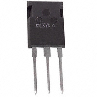
ISOPLUS247TM
ID25 = 165
V
A
8 mW
(Electrically Isolated Back Surface)
RDS(on) =
Single MOSFET Die
trr £ 250 ns
Preliminary data
Symbol
Test Conditions
Maximum Ratings
VDSS
VDGR
T J = 25°C to 150°C
T J = 25°C to 150°C; RGS = 1 MW
100
100
V
V
VGS
VGSM
Continuous
Transient
±20
±30
V
V
ID25
ID(RMS)
IDM
IAR
TC = 25°C (MOSFET chip capability)
External lead (current limit)
TC = 25°C, Note 1
TC = 25°C
165
76
720
180
A
A
A
A
EAR
EAS
TC = 25°C
TC = 25°C
60
3
mJ
J
dv/dt
IS £ IDM, di/dt £ 100 A/ms, VDD £ VDSS
T J £ 150°C, RG = 2 W
5
V/ns
PD
TC = 25°C
400
W
-55 ... +150
150
-55 ... +150
°C
°C
°C
300
°C
2500
V~
5
g
1.6 mm (0.063 in.) from case for 10 s
VISOL
50/60 Hz, RMS
t = 1 min
Weight
Symbol
Test Conditions
Characteristic Values
(TJ = 25°C, unless otherwise specified)
min. typ. max.
VDSS
VGS = 0 V, ID = 3mA
100
V
VGS(th)
VDS = VGS, ID = 8mA
2.0
4.0 V
IGSS
VGS = ±20 V, VDS = 0
IDSS
VDS = VDSS
VGS = 0 V
RDS(on)
VGS = 10 V, ID = 90A
Note 1
±100 nA
TJ = 25°C
TJ = 125°C
IXYS reserves the right to change limits, test conditions, and dimensions.
© 2000 IXYS All rights reserved
G
D
Isolated back surface*
G = Gate
S = Source
D = Drain
* Patent pending
Features
TJ
TJM
Tstg
TL
ISOPLUS 247TM
100 mA
2 mA
8 mW
• Silicon chip on Direct-Copper-Bond
substrate
- High power dissipation
- Isolated mounting surface
- 2500V electrical isolation
• Low drain to tab capacitance(
很抱歉,暂时无法提供与“IXFR180N10”相匹配的价格&库存,您可以联系我们找货
免费人工找货