IXFR18N90P
PolarTMHiPerFETTM
Power MOSFET
VDSS
ID25
RDS(on)
trr
N-Channel Enhancement Mode
Avalanche Rated
Fast Intrinsic Diode
Test Conditions
Maximum Ratings
VDSS
TJ = 25°C to 150°C
900
V
VDGR
TJ = 25°C to 150°C, RGS = 1MΩ
900
V
VGSS
Continuous
± 30
V
VGSM
Transient
± 40
V
ID25
TC = 25°C
10.5
A
IDM
TC = 25°C, Pulse Width Limited by TJM
36
A
IA
EAS
TC = 25°C
TC = 25°C
9
800
A
mJ
dv/dt
IS ≤ IDM, VDD ≤ VDSS, TJ ≤ 150°C
15
V/ns
PD
TC = 25°C
200
W
-55 ... +150
°C
TJM
150
°C
Tstg
-55 ... +150
°C
TL
Maximum Lead Temperature for Soldering
300
°C
TSOLD
Plastic body for 10s
260
°C
VISOL
50/60 Hz, RMS, 1 minute
2500
V~
FC
Mounting force
20..120/4.5..27
N/lb.
5
g
G
D
Isolated Tab
S
G = Gate
S = Source
D
= Drain
Fearures
z
z
z
z
z
z
Silicon Chip on Direct-Copper Bond
(DCB) Substrate
Isolated Mounting Surface
2500V~ Electrical Isolation
Fast Intrinsic Diode
Avalanche Rated
Low Package Inductance
Advantages
z
z
z
Weight
900V
10.5A
Ω
660mΩ
300ns
ISOPLUS247TM
E153432
Symbol
TJ
=
=
≤
≤
High Power Density
Easy to Mount
Space Savings
Applications
z
Symbol
Test Conditions
(TJ = 25°C, unless otherwise specified)
Characteristic Values
Min.
Typ. Max.
BVDSS
VGS = 0V, ID = 1mA
900
VGS(th)
VDS = VGS, ID = 1mA
3.5
IGSS
VGS = ± 30V, VDS = 0V
IDSS
VDS = VDSS
VGS = 0V
RDS(on)
VGS = 10V, ID = 9A, Note 1
V
z
z
z
z
TJ = 125°C
© 2011 IXYS CORPORATION, All Rights Reserved
6.5
V
± 100
nA
DC-DC Converters
Switch-Mode and Resonant-Mode
Power Supplies
Leaser Drivers
DC Choppers
AC and DC Motor Drives
25 μA
1.5 mA
660 mΩ
DS100058A(03/11)
�IXFR18N90P
Symbol
Test Conditions
(TJ = 25°C unless otherwise specified)
Characteristic Values
Min.
Typ.
Max.
gfs
VDS = 20V, ID = 9A, Note 1
6
RGi
Gate input resistance
Ciss
Coss
10
S
1.2
Ω
5230
pF
366
pF
53
pF
40
ns
33
ns
60
ns
44
ns
97
nC
30
nC
40
nC
VGS = 0V, VDS = 25V, f = 1MHz
Crss
td(on)
tr
td(off)
tf
Resistive Switching Times
VGS = 10V, VDS = 0.5 • VDSS, ID = 9A
RG = 2Ω (External)
Qg(on)
Qgs
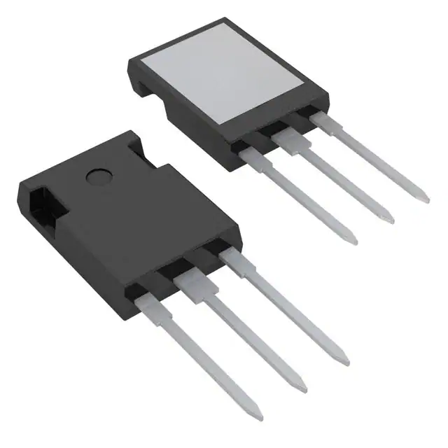
ISOPLUS247TM Outline
VGS = 10V, VDS = 0.5 • VDSS, ID = 9A
Qgd
0.62 °C/W
RthJC
RthCS
0.15
Source-Drain Diode
TJ = 25°C unless otherwise specified)
°C/W
Characteristic Values
Min.
Typ.
Max.
IS
VGS = 0V
18
A
ISM
Repetitive, pulse width limited by TJM
72
A
VSD
IF = IS, VGS = 0V, Note 1
1.5
V
trr
QRM
IRM
Terminals:
Dim.
A
A1
A2
b
b1
b2
C
D
E
e
L
L1
Q
R
1 - Gate
2 - Drain (Collector)
3 - Source (Emitter)
4 - Drain (Collector)
Millimeter
Min. Max.
4.83
5.21
2.29
2.54
1.91
2.16
1.14
1.40
1.91
2.13
2.92
3.12
0.61
0.80
20.80 21.34
15.75 16.13
5.45 BSC
19.81 20.32
3.81
4.32
5.59
6.20
4.32
4.83
Inches
Min. Max.
.190 .205
.090 .100
.075 .085
.045 .055
.075 .084
.115 .123
.024 .031
.819 .840
.620 .635
.215 BSC
.780 .800
.150 .170
.220 0.244
.170 .190
300 ns
IF = 9A, -di/dt = 100A/μs
VR = 100V, VGS = 0V
1.0
μC
10.8
A
Note 1: Pulse test, t ≤ 300μs; duty cycle, d ≤ 2%.
IXYS Reserves the Right to Rhange Limits, Test Conditions, and Dimensions.
IXYS MOSFETs and IGBTs are covered
4,835,592
by one or moreof the following U.S. patents: 4,850,072
4,881,106
4,931,844
5,017,508
5,034,796
5,049,961
5,063,307
5,187,117
5,237,481
5,381,025
5,486,715
6,162,665
6,259,123 B1
6,306,728 B1
6,404,065 B1
6,534,343
6,583,505
6,683,344
6,727,585
7,005,734 B2
6,710,405 B2 6,759,692
7,063,975 B2
6,710,463
6,771,478 B2 7,071,537
7,157,338B2
�IXFR18N90P
Fig. 1. Output Characteristics @ T J = 25ºC
Fig. 2. Extended Output Characteristics @ T J = 25ºC
18
40
VGS = 10V
9V
8V
16
32
14
28
ID - Amperes
12
ID - Amperes
VGS = 10V
9V
36
7V
10
8
6
8V
24
20
16
7V
12
6V
4
8
6V
2
4
5V
5V
0
0
0
1
2
3
4
5
6
7
8
9
0
10
5
10
15
20
25
30
VDS - Volts
VDS - Volts
Fig. 4. RDS(on) Normalized to ID = 9A Value vs.
Junction Temperature
Fig. 3. Output Characteristics @ T J = 125ºC
18
3.0
VGS = 10V
9V
8V
16
VGS = 10V
2.6
R DS(on) - Normalized
ID - Amperes
14
7V
12
10
8
6V
6
I D = 18A
2.2
1.8
I D = 9A
1.4
1.0
4
0.6
5V
2
0
0.2
0
2
4
6
8
10
12
14
16
18
20
22
-50
24
-25
0
VDS - Volts
25
50
75
100
125
150
125
150
TJ - Degrees Centigrade
Fig. 5. RDS(on) Normalized to ID = 9A Value vs.
Drain Current
Fig. 6. Maximum Drain Current vs.
Case Temperature
3.0
12
VGS = 10V
10
TJ = 125ºC
2.2
8
ID - Amperes
R DS(on) - Normalized
2.6
1.8
1.4
6
4
TJ = 25ºC
1.0
2
0.6
0
0
4
8
12
16
20
24
ID - Amperes
© 2011 IXYS CORPORATION, All Rights Reserved
28
32
36
-50
-25
0
25
50
75
TC - Degrees Centigrade
100
�IXFR18N90P
Fig. 7. Input Admittance
Fig. 8. Transconductance
32
18
28
16
TJ = - 40ºC
14
20
TJ = 125ºC
25ºC
- 40ºC
16
12
25ºC
12
g f s - Siemens
ID - Amperes
24
125ºC
10
8
6
8
4
4
2
0
0
3.5
4.0
4.5
5.0
5.5
6.0
6.5
7.0
7.5
8.0
8.5
0
4
8
12
VGS - Volts
Fig. 9. Forward Voltage Drop of Intrinsic Diode
20
24
28
32
Fig. 10. Gate Charge
10
60
VDS = 450V
9
50
I D = 9A
8
I G = 10mA
7
VGS - Volts
40
IS - Amperes
16
ID - Amperes
30
20
TJ = 125ºC
6
5
4
3
2
TJ = 25ºC
10
1
0
0
0.3
0.4
0.5
0.6
0.7
0.8
0.9
1.0
0
1.1
10
20
VSD - Volts
30
40
50
60
70
80
90
100
QG - NanoCoulombs
Fig. 12. Maximum Transient Thermal Impedance
Fig. 11. Capacitance
1
10,000
1,000
Z(th)JC - ºC / W
Capacitance - PicoFarads
Ciss
Coss
0.1
100
Crss
f = 1 MHz
10
0
5
10
15
20
25
30
35
40
VDS - Volts
0.01
0.0001
0.001
0.01
0.1
1
10
Pulse Width - Seconds
IXYS Reserves the Right to Rhange Limits, Test Conditions, and Dimensions.
IXYS REF: F_18N90P(76)10-22-08
�Disclaimer Notice - Information furnished is believed to be accurate and reliable. However, users should independently
evaluate the suitability of and test each product selected for their own applications. Littelfuse products are not designed for,
and may not be used in, all applications. Read complete Disclaimer Notice at www.littelfuse.com/disclaimer-electronics.
�