Preliminary Technical Information
IXFT180N20X3HV
IXFH180N20X3
X3-Class HiPerFETTM
Power MOSFET
VDSS
ID25
= 200V
= 180A
7.5m
RDS(on)
N-Channel Enhancement Mode
Avalanche Rated
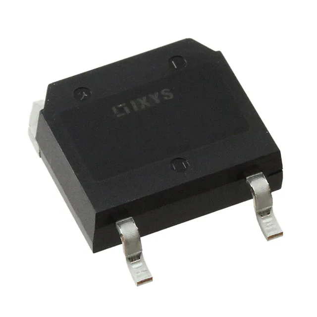
TO-268HV
(IXFT..HV)
G
Symbol
Test Conditions
Maximum Ratings
VDSS
TJ = 25C to 150C
200
V
VDGR
TJ = 25C to 150C, RGS = 1M
200
V
VGSS
Continuous
20
V
VGSM
Transient
30
V
ID25
IL(RMS)
IDM
TC = 25C
External Lead Current Limit
TC = 25C, Pulse Width Limited by TJM
180
160
320
A
A
A
IA
TC = 25C
90
A
EAS
TC = 25C
2.2
J
dv/dt
IS IDM, VDD VDSS, TJ 150°C
20
V/ns
PD
TC = 25C
735
W
-55 ... +150
C
TJM
150
C
Tstg
-55 ... +150
C
300
260
°C
°C
1.13 / 10
Nm/lb.in
4
6
g
g
TJ
TL
TSOLD
Maximum Lead Temperature for Soldering
1.6 mm (0.062in.) from Case for 10s
Md
Mounting Torque (TO-247)
Weight
TO-268HV
TO-247
S
D (Tab)
TO-247
(IXFH)
G
D
S
G = Gate
S = Source
D (Tab)
D
= Drain
Tab = Drain
Features
International Standard Packages
Low RDS(ON) and QG
Avalanche Rated
Low Package Inductance
Advantages
Symbol
Test Conditions
(TJ = 25C, Unless Otherwise Specified)
Characteristic Values
Min.
Typ.
Max.
BVDSS
VGS = 0V, ID = 1mA
200
VGS(th)
VDS = VGS, ID = 4mA
2.5
IGSS
VGS = 20V, VDS = 0V
IDSS
VDS = VDSS, VGS = 0V
V
4.5
Applications
V
100 nA
RDS(on)
25 A
1 mA
TJ = 125C
VGS = 10V, ID = 0.5 • ID25, Note 1
© 2017 IXYS CORPORATION, All Rights Reserved.
6.3
7.5 m
High Power Density
Easy to Mount
Space Savings
Switch-Mode and Resonant-Mode
Power Supplies
DC-DC Converters
PFC Circuits
AC and DC Motor Drives
Robotics and Servo Controls
DS100842C(11/17)
�IXFT180N20X3HV
IXFH180N20X3
Symbol
Test Conditions
(TJ = 25C, Unless Otherwise Specified)
gfs
VDS = 10V, ID = 60A, Note 1
RGi
Gate Input Resistance
Characteristic Values
Min.
Typ.
Max
70
Ciss
Coss
120
S
1.5
10.3
nF
1.7
nF
5.2
pF
810
2540
pF
pF
30
ns
28
ns
100
ns
12
ns
154
nC
50
nC
45
nC
VGS = 0V, VDS = 25V, f = 1MHz
Crss
Effective Output Capacitance
Co(er)
Co(tr)
Energy related
td(on)
Resistive Switching Times
tr
td(off)
tf
Time related
VGS = 0V
VDS = 0.8 • VDSS
VGS = 10V, VDS = 0.5 • VDSS, ID = 0.5 • ID25
RG = 5 (External)
Qg(on)
Qgs
VGS = 10V, VDS = 0.5 • VDSS, ID = 0.5 • ID25
Qgd
0.17 C/W
RthJC
RthCS
TO-247
0.21
C/W
Source-Drain Diode
Symbol
Test Conditions
(TJ = 25C, Unless Otherwise Specified)
Characteristic Values
Min.
Typ.
Max
IS
VGS = 0V
180
A
ISM
Repetitive, pulse Width Limited by TJM
720
A
VSD
IF = 100A, VGS = 0V, Note 1
1.4
V
trr
QRM
IRM
IF = 90A, -di/dt = 100A/μs
120
550
9
VR = 100V
ns
nC
A
Note 1. Pulse test, t 300s, duty cycle, d 2%.
PRELIMINARY TECHNICAL INFORMATION
The product presented herein is under development. The Technical Specifications offered are
derived from a subjective evaluation of the design, based upon prior knowledge and experience, and constitute a "considered reflection" of the anticipated result. IXYS reserves the right
to change limits, test conditions, and dimensions without notice.
IXYS Reserves the Right to Change Limits, Test Conditions, and Dimensions.
IXYS MOSFETs and IGBTs are covered
4,835,592
by one or more of the following U.S. patents: 4,860,072
4,881,106
4,931,844
5,017,508
5,034,796
5,049,961
5,063,307
5,187,117
5,237,481
5,381,025
5,486,715
6,162,665
6,259,123B1
6,306,728B1
6,404,065B1
6,534,343
6,583,505
6,683,344
6,710,405B2
6,710,463
6,727,585
7,005,734B2
6,759,692
7,063,975B2
6,771,478B2 7,071,537
7,157,338B2
�IXFT180N20X3HV
IXFH180N20X3
o
o
Fig. 2. Extended Output Characteristics @ TJ = 25 C
Fig. 1. Output Characteristics @ TJ = 25 C
600
180
VGS = 10V
8V
160
VGS = 10V
7V
9V
500
140
I D - Amperes
I D - Amperes
8V
400
120
100
6V
80
60
300
7V
200
6V
40
100
5V
20
5V
0
0
0
0.2
0.4
0.6
0.8
1
1.2
1.4
1.6
0
5
10
15
VDS - Volts
180
2.8
VGS = 10V
8V
30
VGS = 10V
2.4
RDS(on) - Normalized
7V
140
120
I D - Amperes
25
Fig. 4. RDS(on) Normalized to ID = 90A Value vs.
Junction Temperature
o
Fig. 3. Output Characteristics @ TJ = 125 C
160
20
VDS - Volts
6V
100
80
60
5V
2.0
I D = 180A
1.6
I D = 90A
1.2
40
0.8
20
4V
0.4
0
0
4.5
0.5
1
1.5
2
2.5
-25
0
25
50
75
100
125
VDS - Volts
TJ - Degrees Centigrade
Fig. 5. RDS(on) Normalized to ID = 90A Value vs.
Drain Current
Fig. 6. Normalized Breakdown & Threshold Voltages
vs. Junction Temperature
1.3
VGS = 10V
150
1.2
BVDSS / VGS(th) - Normalized
4.0
3.5
RDS(on) - Normalized
-50
3
o
TJ = 125 C
3.0
2.5
2.0
o
TJ = 25 C
1.5
BVDSS
1.1
1.0
0.9
0.8
0.7
VGS(th)
0.6
1.0
0.5
0.5
0
100
200
300
400
I D - Amperes
© 2017 IXYS CORPORATION, All Rights Reserved.
500
600
-60
-40
-20
0
20
40
60
80
TJ - Degrees Centigrade
100
120
140
160
�IXFT180N20X3HV
IXFH180N20X3
Fig. 7. Maximum Drain Current vs. Case Temperature
Fig. 8. Input Admittance
240
180
VDS = 10V
160
200
External Lead Current Limit
140
160
I D - Amperes
I D - Amperes
120
100
80
60
120
o
TJ = 125 C
80
o
25 C
o
- 40 C
40
40
20
0
0
-50
-25
0
25
50
75
100
125
3.0
150
3.5
4.0
4.5
TC - Degrees Centigrade
5.0
5.5
6.0
6.5
7.0
VGS - Volts
Fig. 9. Transconductance
Fig. 10. Forward Voltage Drop of Intrinsic Diode
250
500
o
TJ = - 40 C
VDS = 10V
400
o
25 C
I S - Amperes
g f s - Siemens
200
150
o
125 C
100
300
200
o
TJ = 125 C
50
100
0
o
TJ = 25 C
0
0
40
80
120
160
200
240
0.2
0.4
0.6
0.8
1.2
1.4
1.6
1.8
Fig. 12. Capacitance
Fig. 11. Gate Charge
100,000
10
VDS = 100V
9
I D = 90A
8
Capacitance - PicoFarads
I G = 10mA
7
VGS - Volts
1.0
VSD - Volts
I D - Amperes
6
5
4
3
2
10,000
Ciss
1,000
Coss
100
Crss
10
f = 1 MHz
1
0
1
0
20
40
60
80
100
120
140
160
QG - NanoCoulombs
IXYS Reserves the Right to Change Limits, Test Conditions, and Dimensions.
1
10
100
VDS - Volts
1,000
�IXFT180N20X3HV
IXFH180N20X3
Fig. 13. Output Capacitance Stored Energy
Fig. 14. Forward-Bias Safe Operating Area
1000
16
RDS(on) Limit
14
25μs
100
10
I D - Amperes
E OSS - MicroJoules
12
8
6
100μs
10
1ms
4
1
o
TJ = 150 C
10ms
DC
o
TC = 25 C
Single Pulse
2
0
0.1
0
1
50
100
Fig.
Transient Thermal
Impedance
15015. Maximum200
1
10
100
1,000
VDS - Volts
VDS - Volts
Fig. 15. Maximum Transient Thermal Impedance
aaaaa
0.3
Z(th)JC - K / W
0.1
0.01
0.001
0.00001
0.0001
0.001
0.01
0.1
1
Pulse Width - Second
© 2017 IXYS CORPORATION, All Rights Reserved.
IXYS REF: F_180N20X3 (27-S202) 6-15-17
�IXFT180N20X3HV
IXFH180N20X3
TO-268HV Outline
PINS:
1 - Gate 2 - Source
3 - Drain
TO-247 Outline
D
A
A2
A2
Q
+
R
A
0P O
+ 0K M D B M
B
E
S
D2
+
D1
D
0P1
1
2
3
4
ixys option
L1
C
E1
L
A1
c
b
b2
b4
e
+ J M C AM
O
PINS: 1 - Gate
2, 4 - Drain
3 - Source
IXYS Reserves the Right to Change Limits, Test Conditions, and Dimensions.
�Disclaimer Notice - Information furnished is believed to be accurate and reliable. However, users should independently
evaluate the suitability of and test each product selected for their own applications. Littelfuse products are not designed for,
and may not be used in, all applications. Read complete Disclaimer Notice at www.littelfuse.com/disclaimer-electronics.
�