HiPerFASTTM IGBT
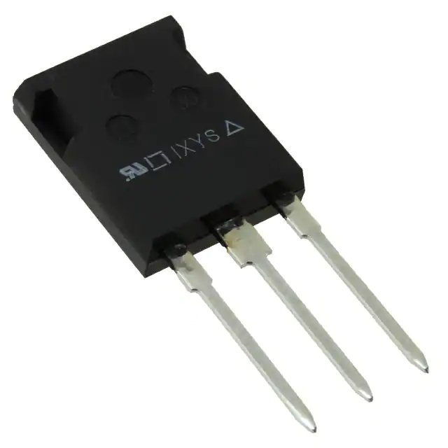
ISOPLUS247TM
IXGR 120N60B
VCES
IC25
(Electrically Isolated Back Surface)
= 600 V
= 156 A
= 2.1 V
VCE(sat)
Symbol
Test Conditions
Maximum Ratings
VCES
TJ = 25°C to 150°C
600
V
VCGR
TJ = 25°C to 150°C; RGE = 1 MΩ
600
V
VGES
Continuous
±20
V
VGEM
Transient
±30
V
IC25
TC = 25°C
156
A
IC110
TC = 110°C
102
A
IL(RMS)
External lead limit
76
A
ICM
TC = 25°C, 1 ms
300
A
G = Gate,
E = Emitter
SSOA
(RBSOA)
VGE = 15 V, TVJ = 125°C, RG = 2.4 Ω
Clamped inductive load
ICM = 200
@ 0.8 VCES
A
* Patent pending
PC
TC = 25°C
520
W
-55 ... +150
°C
TJM
150
°C
Tstg
-55 ... +150
°C
300
°C
TJ
Maximum lead temperature for soldering
1.6 mm (0.062 in.) from case for 10 s
VISOL
50/60 Hz, RMS, t = 1minute leads-to-tab
Weight
2500
V
5
g
ISOPLUS 247
E153432
G
C
Isolated Backside*
E
C = Collector
Features
z
DCB Isolated mounting tab
z
Meets TO-247AD package Outline
z
High current handling capability
z
Latest generation HDMOSTM process
z
MOS Gate turn-on
- drive simplicity
Applications
z
Symbol
Test Conditions
BVCES
IC
= 1 mA, VGE = 0 V
600
VGE(th)
IC
= 1 mA, VCE = VGE
2.5
ICES
VCE = 0.8 • VCES
VGE = 0 V
IGES
VCE(sat)
Characteristic Values
(TJ = 25°C, unless otherwise specified)
min. typ. max.
TJ = 25°C
TJ = 150°C
VCE = 0 V, VGE = ±20 V
IC
= 100A, VGE = 15 V (see note 1)
© 2004 IXYS All rights reserved
V
5.5
V
200
2
µA
mA
±400
2.1
nA
V
Uninterruptible power supplies (UPS)
z
Switched-mode and resonant-mode
power supplies
z
AC motor speed control
z
DC servo and robot drives
z
DC choppers
Advantages
z
Easy assembly
z
High power density
z
Very fast switching speeds for high
frequency applications
DS98744A(08/04)
�IXGR 120N60B
Symbol
Test Conditions
Characteristic Values
(TJ = 25°C, unless otherwise specified)
min. typ. max.
gfs
IC = 60A; VCE = 10 V,
Pulse test, t ≤ 300 µs, duty cycle ≤ 2 %
50
75
S
11000
pF
680
pF
Cres
190
pF
Qg
350
nC
Cies
Coes
Qge
VCE = 25 V, VGE = 0 V, f = 1 MHz
IC = 100A, VGE = 15 V, VCE = 0.5 VCES
Qgc
72
nC
131
nC
td(on)
Inductive load, TJ = 25°°C
60
ns
tri
IC = 100A, VGE = 15 V
VCE = 0.8 • VCES, RG = Roff = 2.4 Ω
45
ns
Eon
td(off)
tfi
Eoff
td(on)
tri
Eon
td(off)
tfi
Eoff
2.4
Remarks: Switching times may increase
for VCE (Clamp) > 0.8 • VCES, higher TJ or
increased RG
Inductive load, TJ = 125°°C
IC = 100A, VGE = 15 V
VCE = 0.8 • VCES, RG = Roff = 2.4 Ω
Remarks: Switching times may increase
for VCE (Clamp) > 0.8 • VCES, higher TJ or
increased RG
mJ
200
360
ns
160
280
ns
5.5
9.6
mJ
60
ns
60
ns
4.8
mJ
290
ns
250
ns
8.7
mJ
RthJC
ISOPLUS 247 OUTLINE
1 Gate, 2 Drain (Collector)
3 Source (Emitter)
4 no connection
Dim.
A
A1
A2
b
b1
b2
C
D
E
e
L
L1
Q
R
Millimeter
Min.
Max.
4.83
5.21
2.29
2.54
1.91
2.16
1.14
1.40
1.91
2.13
2.92
3.12
0.61
0.80
20.80 21.34
15.75 16.13
5.45 BSC
19.81 20.32
3.81
4.32
5.59
6.20
4.32
4.83
0.3 K/W
RthCK
0.15
K/W
IXYS reserves the right to change limits, test conditions, and dimensions.
IXYS MOSFETs and IGBTs are covered by
one or moreof the following U.S. patents:
4,835,592
4,850,072
4,881,106
4,931,844
5,017,508
5,034,796
5,049,961
5,063,307
5,187,117
5,237,481
5,381,025
5,486,715
6,162,665
6,259,123 B1
6,306,728 B1
6,404,065 B1
6,534,343
6,583,505
6,683,344
6,710,405B2
6,710,463
6,727,585
6,759,692
Inches
Min. Max.
.190 .205
.090 .100
.075 .085
.045 .055
.075 .084
.115 .123
.024 .031
.819 .840
.620 .635
.215 BSC
.780 .800
.150 .170
.220 .244
.170 .190
�IXGR 120N60B
Fig. 1. Output Characte ristics
@ 25 ºC
Fig. 2. Extended Output Characte ristics
@ 25 ºC
150
300
VGE = 15V
13V
11V
250
9V
100
I C - Amperes
I C - Amperes
VGE = 15V
13V
11V
125
75
7V
50
25
200
9V
150
7V
100
50
5V
5V
0
0
0.6
0.8
1
1.2
1.4
1.6
1.8
2
2.2
2.4
0
0.5
1
V C E - Volts
Fig. 3. Output Characteristics
@ 125 ºC
VGE = 15V
100
7V
75
50
3
3.5
4
I C = 150A
1.1
1.0
1.0
I C = 100A
0.9
0.9
0.8
25
0.8
5V
0
I C = 50A
0.7
0.6
0.8
1
1.2
1.4
1.6
V CE - Volts
1.8
2
2.2
-50
2.4
-25
0
25
50
75
100
125
150
7.5
8
TJ - Degrees Centigrade
Fig. 5. Collector-to-Em itter Voltage
vs. Gate-to-Em itter voltage
Fig. 6. Input Adm ittance
180
3.6
TJ = 25ºC
3.4
160
3.2
140
3
I C = 150A
2.8
100A
50A
2.6
I C - Amperes
VC E - Volts
2.5
VGE = 15V
1.1
9V
VC E (sat)- Normalized
I C - Amperes
1.2
13V
11V
125
2
V C E - Volts
Fig. 4. Dependence of V CE(sat) on
Tem perature
1.2
150
1.5
2.4
2.2
120
100
TJ = 125ºC
80
25ºC
60
-40ºC
40
2
20
1.8
0
1.6
6
7
8
9
10
11
V G E - Volts
© 2004 IXYS All rights reserved
12
13
14
15
4
4.5
5
5.5
6
6.5
V G E - Volts
7
�IXGR 120N60B
Fig. 8. Dependence of Turn-off
Fig. 7. Transconductance
160
140
TJ = -40ºC
25ºC
E o f f - milliJoules
g f s - Siemens
120
125ºC
100
80
60
9
TJ = 125ºC
8
VGE = 15V
VCE = 480V
7
I C = 100A
6
5
4
40
3
20
2
I C = 50A
1
0
0
20
40
60
80
100
120
140
160
2
180
5
6
7
8
9
Fig. 9. Dependence of Turn-Off
Fig. 10. Dependence of Turn-off
Energy Loss on Tem perature
10
6
R G = 2.7Ω
5
VGE = 15V
5
4
E o f f - milliJoules
TJ = 125ºC
VCE = 480V
4
4
R G - Ohms
Energy Loss on IC
5
3
I C - Amperes
5
E o f f - MilliJoules
Energy Loss on RG
10
TJ = 25ºC
3
3
I C = 100A
R G = 2.7Ω
4
VGE = 15V
4
VCE = 480V
3
3
I C = 50A
2
2
2
2
1
50
55
60
65
70
75
80
I C - Amperes
85
90
95
100
25
Fig. 11. Dependence of Turn-off
45
55
65
75
85
95
TJ - Degrees Centigrade
105 115 125
Fig. 12. Dependence of Turn-off
Sw itching Tim e on RG
700
35
Sw itching Tim e on IC
350
tfi - - - - - -
600
I C = 50A
100A
TJ = 125ºC
500
Switching Time - nanoseconds
Switching Time - nanoseconds
td(off)
VGE = 15V
VCE = 480V
400
300
I C = 100A
50A
200
300
td(off)
tfi - - - - -
250
R G = 2.7Ω
200
VGE = 15V
TJ = 125ºC
TJ = 25ºC
VCE = 480V
150
100
50
100
2
3
4
5
6
R G - Ohms
7
8
9
10
IXYS reserves the right to change limits, test conditions, and dimensions.
50
60
70
80
I C - Amperes
90
100
�IXGR 120N60B
Fig. 13. Dependence of Turn-off
Sw itching Tim e on Tem perature
Fig. 14. Gate Charge
16
350
Switching Time - nanoseconds
I C = 50A
td(off)
I C = 100A
, tfi - - - - -
I C = 100A
12
I G = 10mA
R G = 2.7Ω, VGE = 15V
250
VG E - Volts
VCE = 480V
200
150
I C = 100A
10
8
6
4
50A
100
VCE = 300V
14
300
2
50
0
25
35
45
55
65
75
85
95
TJ - Degrees Centigrade
105 115 125
0
100
200
300
400
500
Q G - nanoCoulombs
Fig. 16. Reverse-Bias Safe
Operating Area
Fig. 15. Capacitance
100000
220
f = 1 MHz
200
160
10000
I C - Amperes
Capacitance - p F
180
C ies
C oes
1000
140
120
100
80
60
TJ = 125ºC
40
R G = 2.7Ω
20
C res
100
dV/dT < 5V/ns
0
0
5
10
15
20
25
V C E - Volts
30
35
40
100 150 200 250 300 350 400 450 500 550 600
V C E - Volts
Fig . 17. M axim u m T r an s ie n t T h e r m al Re s is tan ce
R( t h ) J C - ºC / W
1
0. 1
0 . 01
1
© 2004 IXYS All rights reserved
10
Puls e W idth - millis ec onds
10 0
1000
�Disclaimer Notice - Information furnished is believed to be accurate and reliable. However, users should independently
evaluate the suitability of and test each product selected for their own applications. Littelfuse products are not designed for,
and may not be used in, all applications. Read complete Disclaimer Notice at www.littelfuse.com/disclaimer-electronics.
�