30 A Low-Side RF MOSFET Driver
IXRFD631
Features
Description
• High Peak Output Current
• Low Output Impedance
• Low Quiescent Supply Current
• Low Propagation Delay
• High Capacitive Load Drive Capability
• Wide Operating Voltage Range
• Kelvin Ground
The IXRFD631 is a CMOS highspeed, high-current gate driver
specifically designed to drive
MOSFETs in Class D and E HF
RF applications as well as other
applications requiring ultrafast rise
and fall times or short minimum
pulse widths. The IXRFD631 is an
improved version of the IXRFD630 with a Kelvin ground
connection on the input side to allow use of a common
mode choke to avoid problems with ground bounce. It can
source and sink 30 A of peak current while producing voltage rise and fall times of less than 4 ns and minimum pulse
widths of 8 ns. The input of the driver is compatible with +5
V or CMOS and is fully immune to latch up over the entire
operating range. Designed with small internal delays, cross
conduction or current shoot-through is virtually eliminated.
The features and wide safety margin in operating voltage
and power make the IXRFD631 unmatched in performance
and value.
Applications
• RF MOSFET Driver
• Class D and E RF Generators
• Multi-MHz Switch Mode Supplies
• Pulse Transformer Driver
• Pulse Laser Diode Driver
• Pulse Generator
The surface mount IXRFD631 is packaged in a lowinductance RF package incorporating advanced layout
techniques to minimize stray lead inductances for optimum
switching performance.
Fig. 1- Block Diagram and Truth Table
IN
OUT
0
0
1
1
1
�IXRFD631
30 A Low-Side RF MOSFET Driver
Absolute Maximum Ratings
Parameter
Value
Parameter
Value
Supply Voltage VCC
30 V
Maximum Junction Temperature
150° C
Input Voltage Level VIN
-5 V to VCC + 0.3 V
Operating Temperature Range
-40° C to 85° C
All Other Pins
-0.3 V to VCC +0.3 V
Thermal Impedance (Junction to Case) RӨJC
0.25° C/W
Power Dissipation
TA( AMBIENT) ≤ 25°C
TC (CASE) ≤ 25°C
2W
100 W
Storage Temperature
-40° C to 150° C
Soldering Lead Temperature
(10 seconds maximum)
300° C
Note: Operating the device outside of the “Absolute Maximum Ratings” may cause permanent damage. Typical values indicate conditions for which the device is intended to be functional but do not
guarantee specific performance limits. The guaranteed specifications apply only for the test conditions listed. Exposure to absolute
maximum conditions for extended periods may impact device reliability.
Electrical Characteristics
Unless otherwise noted, TA = 25° C, 8V < VCC < 30V.
All voltage measurements with respect to GND. IXRFD631 configured as described in Test Conditions.
Test Conditions
Min
Typ
3.5
3
Symbol
Parameter
VIH
High input voltage
VCC = 15V for typical value
VIL
Low input voltage
VCC = 15V for typical value
VHYS
Input hysteresis
VIN
Input voltage range
IIN
VOH
VOL
Input current
High output voltage
Low output voltage
0V≤ VIN ≤ VCC
ROH
High output resistance
VCC = 15V IOUT = 100mA
0.25
Ω
ROL
Low output resistance
VCC = 15V IOUT = 100mA
0.17
Ω
IPEAK
Peak output current
VCC = 15V
28
A
IDC
Continuous output current
2.5
A
tR
Rise time
VCC=15V CL=1nF
CL=2nF
4
5
ns
ns
tF
Fall time
VCC =15V CL=1nF
CL=2nF
4
5.5
ns
ns
tONDLY
ON propagation delay
VCC=15V CL=2nF
24
ns
tOFFDLY
OFF propagation delay
VCC=15V CL=2nF
22
ns
PW min
Minimum pulse width
FWHM VCC=15V CL=1nF
8
ns
VCC
Power supply voltage
ICC
Power supply current
Recommended
VCC = 15V VIN = 0V
VCC = 15V VIN = 3.5V
VCC = 15V VIN = VCC
2.8
Max
V
0.8
V
V
VCC + 0.3
V
10
µA
V
V
0.23
-5
-10
VCC - 0.025
0.025
8
15
0
1
0
Units
18
1
3
5
V
mA
mA
mA
CAUTION: These devices are sensitive to electrostatic discharge; follow proper ESD procedures when handling and
assembling.
2
�IXRFD631
30 A Low-Side RF MOSFET Driver
Fig, 2
Fig, 3
Output Resistance vs. Supply Voltage
3.5
0.4
VIH
3
Input Threshold (V)
0.35
Output Resistance (Ω)
Input Threshold vs. Supply Voltage
0.3
ROH
0.25
0.2
ROL
0.15
0.1
VIL
2.5
2
1.5
1
0.5
0.05
0
0
0
5
10
15
20
25
30
35
0
5
Supply Voltage (V)
Fig, 4
7
Fig, 5
20
25
30
Rise Time vs Supply Voltage
8
CLOAD = 4nF
7
CLOAD = 3nF
CLOAD = 4nF
6
5
Rise Time (ns)
Fall Time (ns)
15
Supply Voltage (V)
Fall Time vs Supply Voltage
6
CLOAD = 2nF
4
CLOAD = 1nF
3
C LOAD = 0nF
2
CLOAD = 3nF
5
CLOAD = 2nF
4
CLOAD = 1nF
3
2
1
CLOAD = 0nF
1
0
0
5
10
15
5
20
10
Supply Voltage (V)
Fig, 6
Propagation Delay vs. Supply Voltage
40
7
35
6
30
ON Delay (TDON)
25
OFF Delay
(TDOFF)
20
15
20
Supply Voltage (V)
Fig, 7
Supply Current (mA)
Propagation Delay (ns)
10
15
10
Quiescent Current vs Supply Voltage
5
Input High
4
3
2
Input Low
1
5
0
0
5
10
15
Supply Voltage (V)
20
5
10
15
20
25
Supply Voltage (V)
3
�IXRFD631
30 A Low-Side RF MOSFET Driver
Supply Current vs. Frequency
Vcc = 8V
3.5
3
Supply Current (A)
Supply Current vs. Frequency
Vcc = 12V
Fig, 9
2.5
C = 4nF
6
C = 3nF
5
C = 2nF
2
C = 1nF
1.5
1
Supply Current (A)
Fig, 8
C = 1nF
2
0
0
20
30
C = 2nF
3
1
10
C = 3nF
4
0.5
0
C = 4nF
0
40
10
Frequency (MHz)
Fig, 10
8
20
30
40
Frequency (MHz)
Supply Current vs. Frequency
Vcc = 15V
Supply Current vs Load Capacitance
Vcc = 8V
Fig, 11
2.5
C = 4nF
C = 3nF
6
5
C = 2nF
4
C = 1nF
3
2
2
Supply Current (A)
Supply Current (A)
7
25 MHz
1.5
20 MHz
1
10 MHz
0.5
1
0
5 MHz
0
0
10
20
30
40
0
1
Frequency (MHz)
Supply Current vs Load Capacitance
Vcc = 12V
Fig, 13
3.5
4
3
3.5
Supply Current (A)
Supply Current (A)
Fig, 12
2.5
25 MHz
2
20 MHz
1.5
10 MHz
1
2
3
4
Load Capacitance (nF)
5 MHz
0.5
Supply Current vs Load Capacitance
Vcc = 15V
3
25 MHz
2.5
20 MHz
2
10 MHz
1.5
1
5 MHz
0.5
0
0
0
1
2
Load Capacitance (nF)
3
4
0
1
2
3
4
Load Capacitance (nF)
4
�30 A Low-Side RF MOSFET Driver
Fig, 14
Fig, 15
Peak Sink Current vs. Supply Voltage
Peak Source Current vs. Supply Voltage
50
45
-10
Peak Source Current (A)
Peak Sink Current (A)
0
-20
-30
-40
-50
-60
40
35
30
25
20
15
10
5
-70
0
0
10
20
30
40
0
5
10
Supply Voltage (V)
Fig, 16
Peak Source Current vs. Temperature
Vcc = 15V
Fig, 17
20
25
30
Peak Sink Current vs. Temperature
Vcc = 15V
-20
-22
Source Current (A)
30
Source Current (A)
15
Supply Voltage (V)
35
25
20
15
10
-24
-26
-28
-30
-32
-34
-36
5
-38
0
-40
-50
0
50
-50
100
0
Fig, 18
1.5
50
100
Temperature (°C)
Temperature (°C)
Fig, 19
Rise Time Normalized vs. Temperature
Vcc = 15V
1.5
Fall Time Normalized vs. Temperature
Vcc = 15V
1.4
1.4
1.3
1.3
1.2
1.2
Fall Time
Rise Time
IXRFD631
1.1
1
0.9
1.1
1
0.9
0.8
0.8
0.7
0.7
0.6
0.6
0.5
0.5
-50
0
50
Temperature (°C)
100
-50
0
50
100
Temperature (°C)
5
�30 A Low-Side RF MOSFET Driver
IXRFD631
Fig. 20 Pin Description
Symbol
Function
Vcc
Supply Voltage
IN
Input
IN GND
Input Ground
OUT
Output
Driver Output. For application purposes, this lead is connected
directly to the Gate of a MOSFET
Power Ground
System ground leads. Internally connected to all circuitry, these
leads provide ground reference for the entire device and
should be connected to a low noise analog ground plane for
optimum performance.
GND
Description
Positive power supply voltage input. These leads provide power to
the entire device.
Input signal-TTL or CMOS compatible.
Input Kelvin ground connection
Fig. 21 Test Circuit Diagram
Note: If required, a common mode choke can be added to further stabilize the input. Usually a few nano-henries on a small core will
be sufficient to eliminate threshold variations due to ground bounce.
Fig. 22 Timing Diagram
6
�30 A Low-Side RF MOSFET Driver
IXRFD631
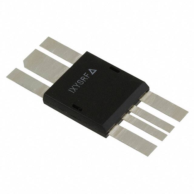
Fig. 23 Package Diagram
Top View
End View
Bottom View
Side View
DCB – Direct Copper Bond under Nickel plate on a Aluminum Nitride substrate and is electrically isolated from any pin.
7
�30 A Low-Side RF MOSFET Driver
Applications Information
Introduction
Circuits capable of very high switching speeds and
high frequency operation require close attention to several important issues. Key elements include circuit loop
inductance, Vcc bypassing, and grounding.
Circuit Loop Inductance
The Vcc to Vcc Ground current path defines the loop
that generates the inductive term. This loop must
be kept as short as possible. The output lead must be
no further than 0.375 inches (9.5 mm) from the gate of
the MOSFET. Furthermore, the output ground leads
must provide a balanced symmetric coplanar ground
return for optimum operation.
Vcc Bypassing
In order to turn a MOSFET on properly, the IXRFD631
must be able to draw up to 30 A of current from the Vcc
power supply in 2-6 ns (depending upon the input capacitance of the MOSFET being driven). Good performance requires very low impedance between the
driver and the power supply. The most common
method of achieving this low impedance is to bypass
the power supply at the driver with a capacitance value
much larger than the load capacitance. Usually, this is
achieved by placing two or three different types of bypassing capacitors, with complementary impedance
curves, very close to the driver itself. (These capacitors
should be carefully selected for low inductance, low
resistance, and high pulse current service.) Care
should be taken to keep the lengths of the leads between these bypass capacitors and the IXRFD631 to
an absolute minimum.
IXRFD631
Output Lead Inductance
Of equal importance to supply bypassing and
grounding are issues related to the output lead inductance. Every effort should be made to keep the
leads between the driver and its load as short and
wide as possible, and treated as coplanar transmission lines. In configurations where the optimum
configuration of circuit layout and bypassing cannot
be used, a series resistance of a few ohms in the
gate lead may be necessary to dampen ringing.
Heat Sinking
For high power operation, the bottom side metalized substrate should be placed in compression
against an appropriate heat sink. The substrate is
metalized for improved heat dissipation, and is not
electrically connected to the device or to ground.
See the technical note “DE-Series MOSFET and
IC Mounting Instructions” on the IXYS Colorado
website at www.ixyscolorado.com for detailed
mounting instructions.
The bypassing should be comprised of several values
of MLC (Multi-Layer Ceramic) capacitors symmetrically
placed on either side of the IC. Recommended values
are 0.01 uF and 0.47 uF for bypass and at least two
4.7 uF tantalums for bulk storage.
Grounding
In order for the design to turn the load off properly, the
IXRFD631 must be able to drain 30 A of current into
an adequate grounding system. There are two paths
for returning current that need to be considered: Path
one is between the IXRFD631 and its load, and path
two is between the IXRFD631 and its power supply.
Both of these paths should be as low in resistance and
inductance as possible, and thus as short as practical.
IXYS Colorado
1609 Oakridge Dr. Suite 100
Fort Collins, CO
Phone: 970-493-1901
Fax: 970-232-3025
Dec. 2012
8
�Disclaimer Notice - Information furnished is believed to be accurate and reliable. However, users should independently
evaluate the suitability of and test each product selected for their own applications. Littelfuse products are not designed for,
and may not be used in, all applications. Read complete Disclaimer Notice at www.littelfuse.com/disclaimer-electronics.
�
很抱歉,暂时无法提供与“IXRFD631-NRF”相匹配的价格&库存,您可以联系我们找货
免费人工找货