IXTR40P50P
PolarPTM
Power MOSFET
VDSS
ID25
RDS(on)
=
=
- 500V
- 22A
260m
P-Channel Enhancement Mode
Avalanche Rated
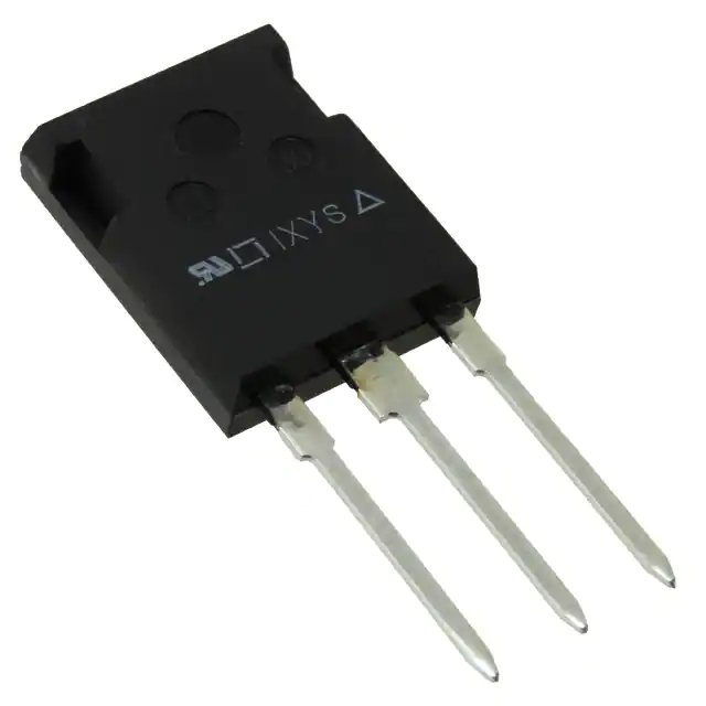
ISOPLUS247
E153432
Symbol
Test Conditions
Maximum Ratings
VDSS
TJ = 25C to 150C
- 500
V
VDGR
TJ = 25C to 150C, RGS = 1M
- 500
V
VGSS
Continuous
20
V
VGSM
Transient
30
V
ID25
TC = 25C
- 22
A
IDM
TC = 25C, Pulse Width Limited by TJM
-120
A
IA
TC = 25C
- 40
A
EAS
TC = 25C
3.5
J
dv/dt
IS IDM, VDD VDSS, TJ 150C
10
V/ns
PD
TC = 25C
312
W
-55 ... +150
150
-55 ... +150
C
C
C
300
260
°C
°C
2500
V~
20..120/4.5..27
N/lb
5
g
TJ
TJM
Tstg
TL
TSOLD
Maximum Lead Temperature for Soldering
1.6 mm (0.062in.) from Case for 10s
VISOL
50/60 HZ ,RMS, t= 1min
Md
Mounting Force
Weight
G
D
Isolated Tab
S
G = Gate
S = Source
D
= Drain
Features
Silicon Chip on Direct-Copper Bond
(DCB) Substrate
- UL Recognized Package
- Isolated Mounting Surface
- 2500V~ Electrical Isolation
Dynamic dv/dt Rating
Avalanche Rated
Fast Intrinsic Diode
The Rugged PolarPTM Process
Low QG
Low Drain-to-Tab Capacitance
Low Package Inductance
Advantages
Symbol
Test Conditions
(TJ = 25C, Unless Otherwise Specified)
Characteristic Values
Min.
Typ.
Max.
BVDSS
VGS = 0V, ID = - 250A
- 500
VGS(th)
VDS = VGS, ID = -1mA
- 2.0
IGSS
VGS = 20V, VDS = 0V
IDSS
VDS = VDSS, VGS = 0V
RDS(on)
VGS = -10V, ID = - 20A, Note 1
V
- 4.5
V
100 nA
TJ = 125C
© 2015 IXYS CORPORATION, All Rights Reserved
Easy to Mount
Space Savings
High Power Density
- 50 A
- 250 A
260 m
Applications
High-Side Switches
Push Pull Amplifiers
DC Choppers
Automatic Test Equipment
Current Regulators
DS99937D4/15)
�IXTR40P50P
Symbol
Test Conditions
(TJ = 25C, Unless Otherwise Specified)
gfs
Characteristic Values
Min.
Typ.
Max.
VDS = -10V, ID = - 20A, Note 1
23
Ciss
VGS = 0V, VDS = - 25V, f = 1MHz
Coss
Crss
td(on)
Resistive Switching Times
tr
VGS = -10V, VDS = 0.5 • VDSS, ID = - 20A
td(off)
RG = 1 (External)
tf
Qg(on)
VGS = -10V, VDS = 0.5 • VDSS, ID = - 20A
Qgs
Qgd
ISOPLUS247 (IXTR) Outline
38
S
11.5
nF
1150
pF
93
pF
37
ns
59
ns
90
ns
34
ns
205
nC
55
nC
75
nC
RthJC
1 - Gate
2,4 - Drain
3 - Source
0.40C/W
RthCS
C/W
0.15
Source-Drain Diode
Symbol
Test Conditions
(TJ = 25C, Unless Otherwise Specified)
Characteristic Values
Min.
Typ.
Max.
IS
VGS = 0V
- 40
A
ISM
Repetitive, Pulse Width Limited by TJM
-160
A
VSD
IF = - 20A, VGS = 0V, Note 1
- 3.0
V
trr
14.5
VR = -100V, VGS = 0V
IRM
Note
477
IF = - 20A, -di/dt = -150A/s
QRM
1:
- 61
ns
C
A
Pulse test, t 300s, duty cycle, d 2%.
IXYS Reserves the Right to Change Limits, Test Conditions, and Dimensions.
IXYS MOSFETs and IGBTs are covered
4,835,592
by one or more of the following U.S. patents: 4,860,072
4,881,106
4,931,844
5,017,508
5,034,796
5,049,961
5,063,307
5,187,117
5,237,481
5,381,025
5,486,715
6,162,665
6,259,123 B1
6,306,728 B1
6,404,065 B1
6,534,343
6,583,505
6,683,344
6,727,585
7,005,734 B2
6,710,405 B2 6,759,692
7,063,975 B2
6,710,463
6,771,478 B2 7,071,537
7,157,338B2
�IXTR40P50P
Fig. 1. Output Characteristics @ TJ = 25ºC
Fig. 2. Extended Output Characteristics @ TJ = 25ºC
-90
-40
VGS = -10V
- 7V
-35
-70
I D - Amperes
-30
I D - Amperes
VGS = -10V
-80
-25
- 6V
-20
-15
- 7V
-60
-50
-40
- 6V
-30
-10
-20
-5
- 5V
-10
- 5V
0
0
0
-1
-2
-3
-4
-5
-6
-7
-8
0
-9
-5
-10
-15
-20
-25
-30
VDS - Volts
VDS - Volts
Fig. 3. Output Characteristics @ TJ = 125ºC
Fig. 4. RDS(on) Normalized to ID = - 20A Value vs.
Junction Temperature
2.4
-40
VGS = -10V
- 7V
-35
VGS = -10V
2.0
-25
RDS(on) - Normalized
I D - Amperes
-30
- 6V
-20
-15
I D = - 40A
1.6
I D = - 20A
1.2
-10
0.8
- 5V
-5
0
0.4
0
-2
-4
-6
-8
-10
-12
-14
-16
-18
-50
-25
0
VDS - Volts
25
50
75
100
125
150
125
150
TJ - Degrees Centigrade
Fig. 5. RDS(on) Normalized to ID = - 20A Value vs.
Drain Current
Fig. 6. Maximum Drain Current vs.
Case Temperature
2.4
-24
VGS = -10V
2.2
-20
TJ = 125ºC
I D - Amperes
RDS(on) - Normalized
2.0
1.8
1.6
1.4
-16
-12
-8
1.2
TJ = 25ºC
-4
1.0
0
0.8
0
-10
-20
-30
-40
-50
-60
I D - Amperes
© 2015 IXYS CORPORATION, All Rights Reserved
-70
-80
-90
-50
-25
0
25
50
75
TC - Degrees Centigrade
100
�IXTR40P50P
Fig. 7. Input Admittance
Fig. 8. Transconductance
-70
70
-60
60
-50
50
25ºC
g f s - Siemens
I D - Amperes
TJ = - 40ºC
-40
TJ = 125ºC
25ºC
- 40ºC
-30
-20
40
125ºC
30
20
-10
10
0
0
-3.5
-4.0
-4.5
-5.0
-5.5
-6.0
-6.5
0
-10
-20
VGS - Volts
Fig. 9. Forward Voltage Drop of Intrinsic Diode
-40
-50
-60
-70
Fig. 10. Gate Charge
-140
-10
-9
VDS = - 250V
-8
I D = - 20A
-120
I G = -1mA
-100
-7
VGS - Volts
I S - Amperes
-30
I D - Amperes
-80
-60
TJ = 125ºC
-40
-6
-5
-4
-3
TJ = 25ºC
-2
-20
-1
0
-0.5
0
-1.0
-1.5
-2.0
-2.5
-3.0
-3.5
-4.0
0
20
40
VSD - Volts
60
80
100
120
140
160
180
200
220
QG - NanoCoulombs
Fig. 12. Forward-Bias Safe Operating Area
Fig. 11. Capacitance
- 1000
100,000
f = 1 MHz
RDS(on) Limit
- 100
10,000
25µs
I D - Amperes
Capacitance - PicoFarads
Ciss
Coss
1,000
100µs
1ms
- 10
10ms
100ms
-1
100
TJ = 150ºC
Crss
DC
TC = 25ºC
Single Pulse
- 0.1
10
0
-5
-10
-15
-20
-25
-30
-35
-40
VDS - Volts
IXYS Reserves the Right to Change Limits, Test Conditions, and Dimensions.
- 10
- 100
VDS - Volts
-1000
�IXTR40P50P
Fig. 13. Maximum Transient Thermal Impedance
Z (th)JC - ºC / W
1
0.1
0.01
0.001
0.00001
0.0001
0.001
0.01
0.1
1
10
Pulse Width - Seconds
© 2015 IXYS CORPORATION, All Rights Reserved
IXYS REF: T_40P50P(B9) 03-06-08-A
�Disclaimer Notice - Information furnished is believed to be accurate and reliable. However, users should independently
evaluate the suitability of and test each product selected for their own applications. Littelfuse products are not designed for,
and may not be used in, all applications. Read complete Disclaimer Notice at www.littelfuse.com/disclaimer-electronics.
�