LDS8160
Dual-Output RGB / 6-Channel WLED Driver
with LED-SenseTM Temperature & Color Compensation
FEATURES
Six PowerLite
Linear LDO current drivers
with 25 mV drop-out in a common cathode
topology with up to 25 mA per channel
LED current programmable from 0 to 25 mA
in 200 linear steps
Three separately controlled driver banks (2
LED each) supports RGB LED applications.
Integrated digital temperature sensor with 100
0
bit ADC; 1 C resolution with 5 C accuracy
TM
LED-Sense * temperature compensation
algorithm continually monitors LED V-I
parameters and adjusts brightness per user
loaded PWM correction
Three integrated PWM generators support
RGB color correction and dimming with 12-bit
resolution and 256 user programmable
logarithmic steps (~ 0.17 dB per step)
2
I C serial programming interface; additional
address pin allows 4 unique slave addresses.
Power efficiency up to 98%; average
efficiency > 80% in Li-ion battery applications
Low current shutdown mode (< 1 µA); Low
current software “standby mode” (< 5 µA)
Soft start and current limiting
LED Short circuit detection and protection, LED
open detection
Thermal shutdown protection
Low EMI.
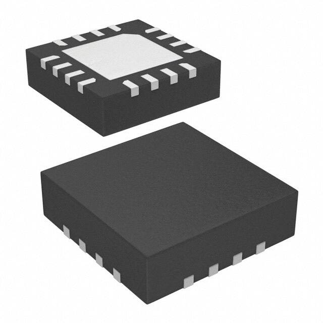
Available in 3 x 3 x 0.8 mm3 16-pin TQFN or ultra
small WCSP 3 x 4 ball grid (0.4mm pitch).
TM
Each channel contains a linear LDO current driver in
a common cathode (i.e., current source) topology.
The LDO drivers have a typical dropout voltage of
25mV at maximum rated current. This provides a low
power and low EMI solution in Li-ion battery
applications without voltage boosting and associated
external capacitors and components.
Three 12-bit PWM generators with “smooth”
logarithmic control support Temperature vs. LED
Luminosity adjustments as well, as RGB color
correction and dimming. The PWM generators are
2
programmable via an I C serial interface. User
programmed 8-bit codes are converted to 12-bit
resolution logarithmic steps of ~ 0.17 dB per step.
The PWM frequency is ~280 Hz to minimize noise.
TM
The LED-Sense temperature compensation engine
includes a multiplexed 10-bit ADC and digital
processing circuits. The algorithm continually
measures the V-I characteristics of the LEDs and an
on-chip temperature diode to determine LED junction
temperatures to within 5ºC accuracy.
APPLICATION
Keypad and Display Backlight
DESCRIPTION
Three user-programmable temperature correction
tables (LUTs) store PWM adjustment codes for every
5ºC increment from -35ºC to 120ºC. These codes
drive the PWM engine to adjust for luminosity
variations and/or high temperature current de-rating.
The three correction LUTs support independent
correction for 3-color RGB applications.
The LDS8160 is a dual-output RGB or 6-channel
white
LED
driver
with
three
temperature
compensation circuits for each bank of two LED
drivers. It supports both RGB LED and WLED
backlighting and keypad in portable applications.
The EN logic input functions as a chip enable. A logic
HIGH applied at EN allows the LDS8160 to respond
2
to I C communication. A serial address pin, SADD,
supports use in multi-target applications. The device
operates from 2.3V to 5.5V.
Three 8-bit DACs set the current level for each LED
bank (A, B, & C) from 0 to 25mA in 0.125mA steps.
The LDS8160 is available in a 0.4mm pitch 12-ball
WCSP or a 3 x 3 x 0.8 mm 16-lead TQFN packages.
Cellular Phones
Digital Still Cameras
PDAs and Smartphones
© 2009 IXYS Corp.
Characteristics subject to change without notice
1
Doc. No. 8160_DS, Rev. N1.0
�LDS8160
TYPICAL APPLICATION CIRCUIT
© 2009 IXYS Corp.
Characteristics subject to change without notice
2
Doc. No. 8160_DS, Rev. N1.0
�LDS8160
ABSOLUTE MAXIMUM RATINGS
Parameter
VIN, LEDx
EN, SDAT, SCLK voltage
Storage Temperature Range
Junction Temperature Range
Soldering Temperature
HBM
ESD Protection Level
MM
Rating
6
V IN + 0.7V
-65 to +160
-40 to +125
300
2
200
Unit
V
V
°C
°C
°C
kV
V
RECOMMENDED OPERATING CONDITIONS
Parameter
VIN
ILED per LED pin
Total Output Current ILOAD
Junction Temperature Range
EN pin Input Voltage @ LP Standby Mode
Rating
2.3 to 5.5
0 – 25
150
-40 to +125
1.8 ± 0.1
Unit
V
mA
mA
°C
V
Typical application circuit with external components is shown on page 1.
ELECTRICAL OPERATING CHARACTERISTICS
(Over recommended operating conditions unless specified otherwise) Vin = 3.6V, Cin = 1 µF, EN = High, TAMB = 25°C
Name
Conditions
Min
2
EN = 1.8 V
LP Standby (no I C clock)
2
EN = VIN
Standby (no I C clock)
Quiescent Current
6 Channels at 100% DC ILOAD = 120 mA
PWMs and Temp
ILOAD = 60 mA
Compensations Active
Shutdown Current
VEN = 0V
LED Current Accuracy
5mA ≤ILED ≤25 mA
LED Channel Matching
(ILED - ILEDAVG ) / I LEDAVG
Line Regulation
2.7 V ≤VIN ≤4.2 V
1
Load Regulation
0.2 V < Vdx < V IN -1.4 V
2
Dropout Voltage
5 mA ≤ILED ≤25 mA
10
PWM Frequency
# of PWM duty cycle steps
Log & Linear Mode
Minimum PWM On Time
PWM resolution
PWM Step Size
of
PWM Adjustment Steps
Log Mode
Linear Mode
Log Mode
Linear Mode
1-x Scale Mode
(~ 0.17 dB per step)
2-x Scale Mode
(~ 0.34 dB per step)
EN Pin
Logic Level
High
Low
1
40
Active mode, EN = VIN
LP Standby
Active Mode or Normal
Standby Mode
+7
-7
+7
-1
3
PWM
0
Steps/5 C
0
0
1
5
1.2
0.4
450
150
Units
µA
µA
mA
mA
µA
%
%
%/V
%/V
mV
Hz
µs
bits
bits
dB
1
5
Input Current Limit
Thermal Shutdown
© 2009 IXYS Corp.
Characteristics subject to change without notice
Max
-7
Temperature Measurement Resolution
Temperature Measurement Accuracy
Input current
Typ
5
125
0.6
0.4
0.5
±1.5
±1.5
2
0.8
25
285
256
13.7
12
8
0.17
ILED/256
C
C
µA
V
mA
°C
Doc. No. 8160_DS, Rev. N1.0
�LDS8160
Name
Thermal Hysteresis
Wake-up Delay Time (EN Raising Edge)
Shutdown Delay Time (EN Falling Edge)
LED Driver PWM Ramp-Up time
2
(from PWM write command via I C)
3
Output short circuit Threshold
Note:
Conditions
Min
Typ
20
0.5
10
Soft Ramp Disabled
Soft Ramping Enabled
(only wake-up)
ILED = 20 mA
Max
Units
ms
250
ms
0.14
V
1. Vdx = Vin – VF,
2. Vdx = Vin – VF, at which I ILED decreases by 10% from set value
3. Minimum LED forward voltage, which will be interpreted as “LED SHORT” condition
I 2C CHARACTERISTICS
Over recommended operating conditions unless otherwise specified for 2.7 VIN 5.5V, over full ambient temperature range -40 to +85ºC.
Symbol
fSCL
tHD:STA
tLOW
tHIGH
tSU:STA
tHD:DAT
tSU:DAT
tR
tF
tSU:STO
tBUF
tAA
tDH
Parameter
SCL Clock Frequency
Hold Time (repeated) START condition
LOW period of the SCL clock
HIGH period of the SCL clock
Set-up Time for a repeated START condition
Data In Hold Time
Data In Set-up Time
Rise Time of both SDAT and SCLK signals
Fall Time of both SDAT and SCLK signals
Set-up Time for STOP condition
Bus Free Time between a STOP and START condition
SCLK Low to SDAT Data Out and ACK Out
Data Out Hold Time
Min
0
0.6
1.3
0.6
0.6
0
100
Max
400
Unit
kHz
µs
µs
µs
µs
µs
ns
ns
ns
µs
µs
µs
ns
0.9
300
300
0.6
1.3
0.9
300
2
Figure 1: I C Bus Timing Diagram
READ OPERATION:
Option 1: Standard protocol sequential read:
S
Slave Address
R
A
Data 0
A
Data 1
From: Reg. m
Reg. m+1
where Reg. m is the last addressed in the write operation register
A
Data 2
Data n
A*
Reg. m+2
Reg. m+n,
P
Option 2: Random access:
S
Slave Address
R
A
Data m
A*
P
From reg. m, where Reg. m is the last addressed in the write operation register
© 2009 IXYS Corp.
Characteristics subject to change without notice
4
Doc. No. 8160_DS, Rev. N1.0
�LDS8160
Option 3: Random access with combined (extended) protocol:
S
Slave Address
W
A
Register Address m
A
Sr
Slave Address
R
A
Data m
A*
P
WRITE OPERATION:
Option 1: Standard protocol sequencial write:
S
Slave Address
W
A
Register Address m
A
Data 0
To: Reg. m
A
Data 1
Reg. m+1
A
Data 2
Reg. m+2
Data k
A*
P
Reg. m+k
At k = 4 data are send to register m and cycle repeats
Option 2: Combined (extended) protocol:
S
Slave Address
W
A
Register Address m
A
Sr
Slave Address
W
A
Data
A*
P
To: Reg. m
S: Start Condition
Sr Start Repeat Condition
R, W: Read bit (1), Write bit (0)
A: Acknowledge (SDAT high)
A*: Not Acknowledge (SDAT low)
P: Stop Condition
Slave Address: Device address 7 bits (MSB first).
Register Address: Device register address 8 bits
Data: Data to read or write 8 bits
- send by master
- send by slave
I2 C BUS PROTOCOL
Standard protocol
Combined protocol:
© 2009 IXYS Corp.
Characteristics subject to change without notice
5
Doc. No. 8160_DS, Rev. N1.0
�LDS8160
WRITE INSTRUCTION SEQUENCE
Standard protocol:
Write Instruction Example - Setting 20mA Current in LEDB1 and LEDB2
REGISTER CONFIGURATION AND PROGRAMMING
ADDRESS
00h
01h
DESCRIPTION
Bank A Current setting
Bank B Current setting
BITS
8
8
02h
Bank C Current setting
8
03h
Channel Enable
6
04h
Global PWM Dimming
8
05h
Bank A PWM Duty Cycle
8
06h
Bank B PWM Duty Cycle
8
07h
Bank C PWM Duty Cycle
8
© 2009 IXYS Corp.
Characteristics subject to change without notice
NOTES
Reg00h – Reg02h data code = (ILED / 0.125 mA) (decimal)
converted into hex format
Bits 5:0 = 1 enables LEDs C2, C1, B2, B1, A2, A1 respectively
(See Table 1).
Both LEDs from one bank should be disabled to minimize
power consumption.
Log mode: (default)
Simultaneously decreases ILED in banks A – C by ~ – 0.17 dB
per step (256 steps).
Data Code 00h = 0 dB dimming, FEh = – 72 dB FFh = OFF
Example: 50% brightness reduction ( – 6dB) requires:
– 6dB / – 0.17dB = 35 (decimal) = 23h steps
Linear Mode:
Simultaneously decreases ILED in banks A – C by subtracting
Global Dimming Code (Reg04h data) from PWM Duty Cycle
Code (Reg05h – Reg07h data)
Data Code 00h = 0 dimming, If Global Dimming Code is equal
or exceeds PWM Duty Cycle Code, ILED = 0 mA.
Log Mode: (default):
~ – 0.17dB dimming per LSB for < 98% Dimming Level (i.e. >
2% Duty Cycle) from full scale;
Refer to 8 to 12 bit conversion curve (Figure 3 and Table
A4.1) for resolution in range 100% to 98% Dimming Level
(i.e. 0% to 2% Duty Cycle).
Data Code 00h = 0% Duty Cycle or 100% Dimming Level,
FFh = 100% Duty Cycle or 0% Dimming Level
Example: 50% brightness reduction ( – 6dB) requires: 255 –
(– 6 dB / – 0.17 dB) = 255 – 35 = 220 (decimal) = DCh steps
Linear Mode:
PWM Duty Cycle resolution ~ 0.39% per LSB
Code 00h = 0% Duty Cycle, FFh = 100% Duty Cycle
6
Doc. No. 8160_DS, Rev. N1.0
�LDS8160
ADDRESS
`
DESCRIPTION
BITS
19h
Digital Test Mode
8
1Ch
LED shorted to GND
6
1Dh
LED Fault Detected
(LED shorted to V IN or
open)
6
1Eh
Configuration register
8
1Fh
Software reset, Standby
8
49h
Ta-Tj Temperature
Offset
8
4Ah
LED shutdown
Temperature
5
4Bh
2-x Table enable and
breakpoint (T-code)
6
50h – 5Fh
60h – 6Fh
70h – 7Fh
A0h
LUT-B
ΔPWM code1[7:4],
ΔPWM code0[3:0] –
ΔPWM code31[7:4],
ΔPWM code30[3:0]
LUT-G
ΔPWM code1[7:4],
ΔPWM code0[3:0] –
ΔPWM code31[7:4],
ΔPWM code30[3:0]
LUT-R
ΔPWM code1[7:4],
ΔPWM code0[3:0] –
ΔPWM code31[7:4],
ΔPWM code30[3:0]
Silicon diode dV F/dT [7:0]
© 2009 IXYS Corp.
Characteristics subject to change without notice
8
NOTES
See Table 2; Bit 5 = 1 sets user-initiated LED short/open
diagnostic
Bits from bit 5 to bit 0 represent LED status for LEDC2 –
LEDA1 respectively. Bit = 1 represents LED shorted to GND
When the corresponding bit in the “faults” detection register,
1Dh, is also High=1, and the associated LED driver current is
disabled.
Bits from bit 5 to bit 0 represent LED status for LEDC2 –
LEDA1 respectively. Bit = 1 represents that an LED Fault is
detected. If the corresponding bit in register 1Ch is also High
=1, than the LED is shorted to ground and current driver is
disabled. If the corresponding bit in register 1Ch is Low=0 than
the LED is either shorted to V IN or open
See Table 3
See Table 4
Two 4-bit compensation offsets between Ta and Tj:
Bit [7:4] = temperature offsets for LED temperature
Bit [3:0] = temperature offset for Silicon diode temperature
0
Each LSB = 5°C; temperature adjustment range from -40 C to
0
+35 C
Code 1000 in either nibble = -40ºC offset; Code 0111 in either
nibble = +35ºC offset. See Tables 5 and 6
Defines T-code, at which LED current shuts down per LED
vendor de-rating specification (see Table 7); Factory default
0
value = 11100 (bin) = 1Ch represents 105 C.
Bit 5 = 1 – enable 2-x scale LUT ΔPWM code correction (derating) starting at the breakpoint set by T-code (bits 4:0)
Bit 5 = 0 – 1-x scale (default) for entire temperature range
Bit [4:0] defines T-code, where temperature derating starts, or
where 2-x scaling begins (see Table 7)
1-x scale is ~ ± 0.17dB per step
2-x scale is ~ ± 0.34dB per step
2
Two LUT words per I C address.
Each word contains two 4-bit numbers representing of ΔPWM
codes.
See Table 8 and Appendix 1 for LUT programming.
Coding is different for Logarithmic and Linear Modes.
8
See above:
8
See above:
8
Silicon diode VF temperature coefficient :
Factory recommended value = -1.71 mV/°C = 001 10110
(bin) = 36h,
where bits from bit 7 to bit 5 represent integer part [1(decimal)
= 001 (bin)], and bits from bit 4 to bit 0 – fractional part [0.710 /
0.03125 = 22 (decimal) = 10110 (bin)]
7
Doc. No. 8160_DS, Rev. N1.0
�LDS8160
ADDRESS
A2h
DESCRIPTION
LED-A dVF/dT [7:0]
BITS
8
A4h
LED-B dVF/dT [7:0]
8
A6h
LED-C dV F/dT [7:0]
8
C0h
Silicon diode η[7:0]
8
D0h
LED Tj offset [4:0]
5
D2h
Silicon diode Ta offset
[4:0]
5
D4h
Silicon diode Rs offset
[7:0]
8
D6h
LED-A Rs offset [7:0]
8
D8h
LED-B Rs offset [7:0]
8
DAh
LED-C Rs offset [7:0]
8
DCh
TMIN offset [7:0]
8
NOTES
User-loaded V F temperature coefficient for LEDs used at
Banks A, B, C respectively.
Negative tracking assumed with temperature;
Bits from bit 7 to bit 5 represent integer part and
bits from bit 4 to bit 0 - fractional part of the coefficient
0
Example: Temperature coefficient = -2.26 mV/ C;
Bit 7 – bit 5 = 2 (decimal) = 010 (bin), and
Bit 4 – bit 0 = INT{0.26 / 0.03125} = 8 (decimal) = 01000 (bin)
User loads 010 01000 (bin) = 48h = -2.25 (closest setting)
Silicon diode η(eta) or non-ideality factor:
Factory recommended loaded value = 1.0000 =
01000000(bin) = 40h
Bits from bit 7 to bit 6 represent integer part and
bits from bit 5 to bit 0 - fractional part (resolution = 0.015625
per LSB)
Example: η= 1.000;
Bit 7 – bit 6 = 1 (decimal) = 01 (bin), and
Bit 5 – bit 0 = INT{0.000 / 0.015625} = 0 (dec) = 000000 (bin)
User loads 01 000000 = 40h = 1.0000
LED Tj offset from Ta (user-loaded) – correction from ambient
temperature to LED junction temperature.
Factory default = 04h
Accounts for LED package thermal characteristics. See
Appendix 3 for details.
Silicon diode Tj offset from Ta – correction from ambient
temperature to Silicon diode junction temperature. Accounts
for LDS8160 package thermal characteristics. Factory default
= 02h
Silicon diode series resistance offset
Factory recommended loaded value = 04h (4 decimal) = ~ 68
Ω=Rs-si
-6
Formula (decimal) = 8192 x [(Rs-si x 8 x 10 A)/1.14 V]
Rs offset (user-loaded) for Banks A, B, and C LEDs for
specific LEDs used.
User loads per LED used. (1/slope of high current region of
LED I-V characteristic).
-4
Formula (decimal) = 8192 x [(Rs Ωx 8 x 10 A) / 1.14V]LEDs
Offset to establish minimum T-code = 0
0
This offset insures that -35C will equal T-code = 0. Factory
default supplied (237 decimal = EDh)
Table 1
Register
Address
03h
Bit 7
LED OT Flag
1 = OT
© 2009 IXYS Corp.
Characteristics subject to change without notice
Bit 6
N/A
Channel Enable Register
Bit 5
Bit 4
Bit 3
Enable
Enable
Enable
C2
C1
B2
8
Bit 2
Enable
B1
Bit 1
Enable
A2
Bit 0
Enable
A1
Doc. No. 8160_DS, Rev. N1.0
�LDS8160
Table 2
Register
Address
19h
Bit 7 Bit 6
Factory
Only
0*
Bit 5
Diagnostics
Request
0*
0*
Digital Test Modes Register
Bit 4
Bit 3
Bit 2
PWM Ramp
PWM Fast
Factory
Bypass = 1
Ramp = 1
Only
PWM Slow
0*
0*
Ramp = 0*
Bit 1
Post ADC
Filter On =1
Filter
Bypass=0*
Bit 0
Factory
Only
0*
Note: *) Value by default
Table 3
Register
Address
1Eh
Configuration Register
Bit 5
Bit 4
Bit 3
Bit 2
Bit 1
Bit 0
Factory
dT adjust Soft Start
RGB mode
PWMs in
Silicon
PWM starts
LP standby
Only
disable PWM Ramp
with 3 LUTs
Linear
Diode
simultaneously
mode
(Leave set
= 1*
disabled
(3 PWM) =1* mode = 1
enable = 1
=1
=1
to 0)
=1
Normal
WLED mode
PWMs in
Silicon
PWMs
dt _adjust Soft Ramp
standby
with 1 LUT Logarithmic
Diode
shifted by
enabled
enabled
0*
mode
0
(1 PWM) = 0 mode = 0*
disable = 0*
120 = 0*
=0
= 0*
= 0*
Bit 7
Bit 6
Note: *) Value by default
Table 4
Register
Address
1Fh
Note:
Bit 7
Bit 6
Bit 5
Software
reset = 1
Standby
mode = 1
Temperature
request = 1
Normal
operation
= 0*
Normal
operation
= 0*
Normal
operation
= 0*
Control Register
Bit 4
Bit 3
Custom
Calibration
OSC trim
request = 1
=1
Factory
Normal
preset
operation
value =
= 0*
0*
Bit 2
Bit 1
Bit 0
Osc trim 2
**
Osc trim 1
**
Osc trim 0
**
*) Value by default
**) Trim code defined by customer
Bit 7 = 1 — Software reset: resets device, all registers reset/cleared.
Bit 6 = 1 — Standby (oscillator disabled, all registers retain programmed values.)
Table 5: Ta-Tj Temperature Gradient Offset
( set offset code to match reference De-rate point in LUT from LED Tj to Ta. Typically LED and Si are equal)
Register
Address
49h
Note:
Bit 7
LED
Offset 3
0*
Bit 6
LED
Offset 2
0*
Bit 5
LED
Offset 1
0*
Control Register
Bit 4
Bit 3
LED
Si Diode
Offset 0
Offset 3
0*
0*
Bit 2
Si Diode
Offset 2
0*
Bit 1
Si Diode
Offset 1
0*
Bit 0
Si Diode
Offset 0
0*
*) Value by default
© 2009 IXYS Corp.
Characteristics subject to change without notice
9
Doc. No. 8160_DS, Rev. N1.0
�LDS8160
Table 6: Offset Codes for Tj-Ta Temperature Gradient Offset (both LED and Si per Table 5).
Temperature
0
Offset C
(Ta-Tj)
-40
-35
-30
-25
Bit3 –
Bit 0
1000
1001
1010
1011
Temperature
0
Offset C
(Ta-Tj)
-20
-15
-10
-5
Temperature
0
Offset C
(Ta-Tj)
0
5
10
15
Bit3 –
Bit 0
1100
1101
1110
1111
Bit3 –
Bit 0
0000
0001
0010
0011
Temperature
0
Offset C
(Ta-Tj)
20
25
30
35
Bit3 –
Bit 0
0100
0101
0110
0111
Table 7: T-code values vs. Temperature (for registers 4Ah and 4Bh)
Temperature,
0
C
-35
-30
-25
-20
-15
-10
-5
0
Bit4 – Bit 0
00000
00001
00010
00011
00101
00101
00110
00111
Temperature,
0
C
5
10
15
20
25
30
35
40
Bit4 – Bit 0
01000
01001
01010
01011
01100
01101
01110
01111
Temperature,
0
C
45
50
55
60
65
70
75
80
Bit4 – Bit 0
10000
10001
10010
10011
10100
10101
10110
10111
Temperature,
0
C
85
90
95
100
105
110
115
120
Bit4 – Bit
0
11000
11001
11010
11011
11100
11101
11110
11111
Table 8: ΔPWM Code Allocation
Register
Address
50h, 60h, 70h
51h, 61h, 71h
52h, 62h, 72h
53h, 63h, 73h
54h, 64h, 74h
55h, 65h, 75h
56h, 66h, 76h
57h, 67h, 77h
Data bits
7– 4
3–0
ΔPWM code for
0
temperature, C
-30
-35
-20
-25
-10
-15
0
-5
10
5
20
15
30
25
40
35
Register
Address
58h, 68h, 78h
59h, 69h, 79h
5Ah, 6Ah, 7Ah
5Bh, 6Bh, 7Bh
5Ch, 6Ch, 7Ch
5Dh, 6Dh, 7Dh
5Eh, 6Eh, 7Eh
5Fh, 6Fh, 7Fh
Data bits
7 –4
3– 0
ΔPWM code for
0
temperature, C
50
45
60
55
70
65
80
75
90
85
100
95
110
105
120
115
Table 9: ΔPWM Codes vs. Number of Adjustment Steps
Number of
steps
Not Valid
-7
-6
-5
Binary
Code
1000
1001
1010
1011
Number of
steps
-4
-3
-2
-1
© 2009 IXYS Corp.
Characteristics subject to change without notice
Binary
Code
1100
1101
1110
1111
Number of
steps
0
1
2
3
10
Binary
Code
0000
0001
0010
0011
Number of
steps
4
5
6
7
Binary
Code
0100
0101
0110
0111
Doc. No. 8160_DS, Rev. N1.0
�LDS8160
PROGRAMMING EXAMPLES
Operation
Set 18 mA current at Bank LEDA
Set 20 mA current at LEDA, 18 mA at LEDB, and 15 mA at LEDC
banks (assuming address at 00h and consecutive writes)
Turn LEDs A1, B1 and C1 on, all others off
Turn LEDs A2, B2, and C2 on, all others off
Turn all LEDs on
Decrease brightness at 50% (-6 dB) at all three channels
simultaneously (in logarithmic mode only)
Decrease brightness at 75% (-12 dB) at all three channels
simultaneously (in logarithmic mode only)
Restore full brightness at all three channels simultaneously
Set Bank B PWM duty Cycle at 50% (-6 dB) in logarithmic mode
Set Bank B PWM duty Cycle at 50% in linear mode
Short/open LED diagnostic request
Read out LED short to GND status
Read out LED short to VIN /open status
Set WLED Mode with 1 PWM generator in linear mode, soft start
disabled, and LP standby mode
Set Standby Mode
Resume normal operation from standby mode
Calibration request (conduct temperature calibration; wait >=16ms)
0
Set LEDs in shutdown mode at temperature above 85 C
0
Set 2-x scale de-rating at temperature equal or above 55 C
Software Reset (to default values) and/or clear of all registers
Note:
Register
Address
00h
90h
Command
(hex)
XX 00 90
00h
A0h 90h 78h
XX A0 90 78
03h
03h
03h
15h
24h
3Fh
XX 03 15
XX 03 24
XX 03 3F
04h
23h
XX 04 23
04h
47h
XX 04 47
04h
06h
06h
19h
1Ch
1Dh
00h
DCh
80h
20h
XX 04 00
XX 06 DC
XX 06 80
XX 19 20
XX 1C YY
XX 1D YY
1Eh
43h
XX 1E 43
1Fh
1Fh
1Fh
4Ah
4Bh
1Fh
40h
00h
10h
18h
32h
80h
XX 1F 40
XX 1F 00
XX 1F 10
XX 4A 18
XX 4B 32
XX 1F 80
Register Data
XX – The LDS8160 I2C customer-selected slave address followed by binary 0 for write command, i.e. if I 2C slave address is
001 0001 (see Table 10), XX = 0010 0010 (bin) = 22h
YY – The LDS8160 I2C customer-selected slave address followed by binary 1 for read command, i.e. if I 2C slave address is
001 0001 (see Table 10), YY = 0010 0011 (bin) = 23h
© 2009 IXYS Corp.
Characteristics subject to change without notice
11
Doc. No. 8160_DS, Rev. N1.0
�LDS8160
PIN DESCRIPTION
Pin #
1
2
3
4
6
8
9
10
11
12
13
14
15
5, 7, 16
PAD
Name
SCLK
SDAT
SADD
GND
EN
LEDC2
LEDC1
LEDB2
LEDB1
LEDA2
LEDA1
V IN
TST
NC
PAD
Function
2
I C Serial clock input
2
I C Serial data input/output
2
I C Serial interface Addresses Programming
Ground Reference
Device enable (active high)
LEDC2 anode terminal
LEDC1 anode terminal
LEDB2 anode terminal
LEDB1 anode terminal
LEDA2 anode terminal
LEDA1 anode terminal
Power Source Input; connect to battery or supply
Test pin
Not connect (no internal connect to the device)
Connect to GND on the PCB
Top view: TQFN 16-lead 3 X 3 mm
PIN FUNCTION
2
VIN is the supply pin. A small 1μF ceramic bypass
capacitor is required between the VIN pin and ground
near the device. The operating input voltage range is
from 2.3 V to 5.5 V.
SADD is I C Serial interface Addresses Programming
2
pin that allows choice of one of four I C addresses
preprogrammed in device.
GND is the ground reference for internal circuitry.
The pin must be connected to the ground plane on
the PCB.
EN is the enable input for the device. Guaranteed
levels of logic high and logic low are set at 1.3 V and
0.4V respectively. When EN is initially taken high, the
device becomes enabled and can communicate
2
through I C interface after a 500 µsec wakeup
(initialization) period.
LEDA1 – LEDC2 provide the internal regulated
current sources for each of the LED anodes. These
pins enter high-impedance zero current state
whenever the device is in shutdown mode.
2
SDAT is the I C serial data line. This is a bidirectional
line allowing data to be written into and read from the
registers of the LDS8160
PAD is the exposed pad underneath the package.
For best thermal performance, the tab should be
soldered to the PCB and connected to the ground
plane
2
SCLK is the I C serial clock input.
TST is a test pin used by factory only. Leave it
floating (no external connection)
© 2009 IXYS Corp.
Characteristics subject to change without notice
12
Doc. No. 8160_DS, Rev. N1.0
�LDS8160
BLOCK DIAGRAM
Figure 2: LDS8160 Functional Block Diagram
VIN
All Drivers 0 to 25 mA
Vin to
al l
Drivers
OverTemp
I2C Interface
Top Level Control
diagnostics
Shorted LED
Open LED
LED Calibration
Soft Start control
SCLK
PWMA
Calibrated
Reference
Currents
and
ADC bias
currents
Bandgap
Voltage
Reference
1.2V
SDAT
DA1
PWMA
1.2V
32
ADC
10 bit SAR
10
Digital Temperature
Sensor / Abritrator
DA2
Pre-Scale
8x, 1x, or 1/4x
PWMB
Si Iforce
LED Iforce
DB1
SADD
1 0 uA
2 uA 1 mA
0.2 mA
Blue LUT
PWMB
OTP
Green LUT
DB2
Si PNP
temp diode
Trim
PWMC
Red LUT
Temp
Compensation
Tables
Temp to PWM
adjust LUTs
OTP
Driver
GND
Vin to 1.8V LDO
for digital core
to PWMA
PWMB (green)
8 bit to 12 bit (log) PWM
Generator
to PWMB
PWMC (red)
8 bit to 12 bit (log) PWM
Generator
1.8V
Gnd
PWMA (blue)
8 bit to 12 bit (log) PWM
Generator
To top control
DC1
PWMC
to PWMC
DC2
to top control & dig processing
Vin
1.2V
POR
Start Up
Oscillator & Clock Generator
~ 1.2 MHz
Vin
EN
BASIC OPERATION
When EN is taken HIGH, a soft-start power-up
sequence begins and performs internal circuits reset
that requires less than 100 µs.
The LDS8160 may operate in follow modes:
a) Normal Operation Mode
b) Custom Operation Modes
c) Normal Standby Mode
d) Low Power (LP) Standby Mode
e) Programming Modes
f) Shutdown Mode
An initialization sequence then begins taking less
than 10 ms. This sequence determines the user2
selected I C slave address, loads factory
programmed settings, and conducts initial diagnostics
for open/shorted LEDs.
2
NORMAL OPERATION MODE
At this point, the I C interface is ready for
communication and the LDS8160 may be userprogrammed. Upon programming completion for all
required initial parameters and features’ settings, a
calibration command is given by setting bit 4 of the
At power-up, V IN should be in the range from 2.3 V to
5.5 V (max). If V IN is slow rising, EN pin should be
logic LOW at least until VIN reaches 2.3 V level.
© 2009 IXYS Corp.
Characteristics subject to change without notice
13
Doc. No. 8160_DS, Rev. N1.0
�LDS8160
Control Register (1Fh) HIGH. This starts the
TM
calibration sequence of the LDS8160 LED-Sense
temperature compensation circuits. The calibration
process takes approximately 16 ms.
02h) and data that represents the code for the
desired LED current. (See Table 10 for accessible
slave addresses.)
Code for LED current is determined as ILED/0.125 mA
in hex format, i.e. 20 mA current code = 20/0.125 =
160 (dec) = A0h.
The user can then additionally program the DC
current and PWM duty cycles for the LEDs. A PWM
ramp-up sequence occurs after the writing to the
PWM registers. This ramp-up delay in less than 250
ms in the default soft-start ramp mode, or can be 64
ms using the optional fast (4x) ramp mode (bit 3 of
Register 19h = HIGH). A further option is available to
bypass the soft-start PWM ramp mode entirely and
the initialization time will be reduced to just the
calibration sequence time of ~ 16ms. The initial softstart ramp mode can be bypassed by setting bit 4 of
register 19h HIGH.
The LDS8160 maximum current should not exceed
25 mA per LED (i.e. current code should not exceed
200 (dec) = C8h) to meet all electrical specifications.
To turn LEDs ON/OFF register 03h should be
addressed with data that represents the desired
combination of LEDs turned ON/OFF (see Table 1);
i.e. if LEDC1, LEDC2, LEDA1, LEDA2 should be ON,
and LEDB1, LEDB2 should be OFF, binary code that
should be written into register 03h is 110011 (bin) =
33h.
The calibration parameters for the temperature
measurement
engine
and
all
customer-set
parameters remain intact until the part is reset or
powered-down. Additionally, the user can re-calibrate
LDS8160 during times when LED currents are
brought to zero and the system is thermally stabilized
by programming the calibration command bit as
discussed.
The LDS8160 allows two ways for LED current
setting. One of them is using registers 00h – 02h
(static mode) and other one by using the PWM signal
to decrease average LED current value set by these
registers (dynamic mode).
For dynamic mode, the LDS8160 integrates 3 digital
PWM generators that operate at a frequency of ~ 285
Hz. In Logarithmic Mode, the PWM generators are
12-bit resolution and can be programmed with an 8bit code to provide 256 internally mapped 12-bit
logarithmic duty cycle steps to adjust the dimming
level. In Linear Mode, the PWM generates 256 linear
duty cycle steps to adjust the dimming levels from the
user programmed 8-bit code.
Factory preset values (upon completion of the powerup initialization but prior to user programming) are as
follow (see Table3):
a) All LEDs are disabled and ILEDA, B, C = 0;
b) RGB mode with three independent
Luminosity vs. Temperature correction tables
(LUTs) selected and three PWM generators;
The advantage of PWM dimming is stable LED color
temperature / wavelength that are determined by the
maximum LED current value set by registers 00h –
02h.
c) PWM dimming control in Logarithmic Mode
0
with PWM generators running by 120 phase
shift;
d) LED temperature compensation enabled with
LUTs
in
Logarithmic
Mode
Soft
start/shutdown enabled;
To use the dynamic PWM mode for LED current
setting, the maximum ILED value should be first set by
registers 00h – 02h as described above in static
mode and the desired PWM dimming should be set
by registers 05h – 07h. In Logarithmic Mode, set by
default, dimming resolution is approximately -0.17 dB
per step with 0dB dimming, or 100% duty cycle, at
th
the 256 step.
e) Internal Diode for temperature compensation
is enabled
f)
LEDs are used as sensors for temperature
compensation control.
Global PWM Dimming
LED Current Setting
The LDS8160 allows Global PWM Dimming control of
all three banks in the RGB Logarithmic mode, set by
default. It is convenient, because it allows the user to
simultaneously change LED brightness equally
across to all three channels independent of the
maximum static current setting (registers 00h, 01h
and 02h) in a particular channel.
Current setting registers 00h – 02h should be
2
programmed using I C interface and desired LEDs
should be enabled using register 03h before LEDs
turn on.
2
The standard I C interface procedure is used to
2
program ILED current (see section “I C INTERFACE”).
LDS8160 should be addressed with slave address
chosen followed by register address (00h, 01h, or
© 2009 IXYS Corp.
Characteristics subject to change without notice
14
Doc. No. 8160_DS, Rev. N1.0
�LDS8160
For example, to decrease LED brightness by 50%
(-6dB) at all three LED banks, Global PWM Dimming
data code written in register 04h should be 6/0.17 =
35 (decimal) = 23h (see Figure 6: Global Dimming in
Logarithmic Mode in percent vs. register 04h data
(0% dimming = full LED brightness).
LUT corrections codes are added/subtracted to/from
the user-set duty cycle/dimming codes (dynamic
and/or global) for the channel to correct LED
brightness.
The LDS8160 integrates a 10-bit ADC and digital
processing to determine LED temperatures
approximately every 2.5 seconds. The proprietary
TM
LED-Sense algorithm allows direct measurement of
LED junction temperatures on the LEDA1, LEDB1,
and LEDC1 driver channels. Additionally an on-chip
silicon temperature sensing diode is also measured
to enhance temperature estimation accuracy.
The LDS8160 integrates temperature measurement
and compensation processing to maintain stable LED
brightness across varying ambient temperature and
de-rate power dissipated by LEDs, if the LED die
temperature exceeds a preset value.
Figure 3: Dynamic Mode Dimming in Logarithmic
Mode in dB vs. registers 05h – 07h data
(0dB dimming = full LED brightness)
Figure 5: Global Dimming in Logarithmic Mode in
dB vs. register 04h data
(0dB dimming = full LED brightness)
Figure 4: Dynamic Mode Dimming in Logarithmic
Mode in percent vs. registers 05h – 07h data
(0% dimming = full LED brightness)
Figure 6: Global Dimming in Logarithmic Mode in
percent vs. register 04h data
(0% dimming = full LED brightness)
Measured temperatures are encoded into 5-bit
0
T-codes representing 5 C temperature intervals from
0
-35 to +120 C. The measured T-code addresses
stored ΔPWM adjustment codes to adjust the
dimming level and therefore average current through
the LEDs. The user loads specific ΔPWM codes into
the LUTs to maintain constant average current and
therefore luminosity over temperature.
© 2009 IXYS Corp.
Characteristics subject to change without notice
In normal operation mode, the LDS8160 senses the
LED temperatures from all 3 available channels when
in the default RGB (3 channel) mode, or only from the
LEDA1 channel when used in the WLED (single
channel) mode.
15
Doc. No. 8160_DS, Rev. N1.0
�LDS8160
Temperature vs. PWM Duty Cycle Profiles
temperature with maximum
temperature of 85ºC.
The user must load the PWM correction look up
tables (LUTs) prior to operation. For the LDS8160 all
three tables, LUT-B, LUT-G and LUT-R require
loading (even if using same data for a WLED
application) with the user correction profiles prior to
operation. For RGB applications, LUT-B which drives
LEDA1 And LEDA2 respectively should be assigned
as the Blue color channel. LUT-G which drives
LEDB1 and LEDB2 should be assigned as the Green
color channel, and LUT-R which drives LEDC1 and
LEDC2 should be the RED channel.
ambient
operating
Figure 8: Luminosity vs. LED Forward Current
for Nichia NSSM038AT-E RGB LED
The correction tables are based upon LED vendor
characteristics for luminosity vs temperature and
current, LED current de-rating specifications, and
user system thermal design parameters. Figure 7
shows an actual Luminosity vs. Temperature curve of
the NSSM038AT-E RGB LED available from Nichia
Corp.
~ linear from
0 -30 mA
0
Figure 7: Luminosity vs. Temperature curve
(NSSM038AT-E RGB LED from Nichia)
Figure 9: Total power (combined R, G, and B
diodes) power de-rating curve
(NSSM038AT-E RGB LED from Nichia)
Figure 8 shows the typical LED characteristic of
decreasing illumination over temperature, but each
color changes differently. This results in white light
color shifts over temperature if not accounted for. It is
typical to see RED LED Luminosity vs Temperature
to change by ± 50% relative to the 25ºC level.
Figure 10 shows the final plot of typical LDS8160
PWM LUT correction profiles that could be
programmed by the user to adjust for this RGB LED.
This accumulated correction takes into account both
the Luminosity vs Temperature variations and the
adjustments to meet the higher temperature power
de-rating specification.
Figure 9 shows that luminosity is linearly dependent
with LED forward currents ≤30 mA. Therefore loss of
LED luminosity over temperature can be
compensated for by associated increases in LED
current.
Given the 5ºC increments of the temperature
adjustment intervals for the LDS8160, the currents
are slowly ramped to equalize loss of light output
before the de-rating profile begins. Once de-rating
begins, the PWM duty cycle is reduced, lowering LED
driver current, to insure meeting and regulating to the
desired maximum operating temperature.
Figure 9 gives the total RGB Power de-rating
specification for the same Nichia NSSM038AT-E
RGB LED. Total power is the combined power (VF x
IF) of each color LED. This curve specifies the
maximum RGB LED power that insures not
exceeding
the
maximum
specified
junction
© 2009 IXYS Corp.
Characteristics subject to change without notice
16
Doc. No. 8160_DS, Rev. N1.0
�LDS8160
Figure 10: Example LDS8160 Accumulated PWM
Correction Curves for Nichia NSMM038AT-E RGB
LED for ILED nominal (R, G, & B) = 15 mA @ 25ºC
The LDS8160 allows user to choose between one of
2
four preprogrammed I C addresses by connecting
SADD pin (#3) either to ground, SCLK, SDAT or VIN
pin (see Table 10). Consult factory about other
addresses available.
2
Table 10: LDS8160 I C Slave Addresses
SADD pin
connected to
Ground
SCLK
SDAT
VIN
2
I C Address
Binary code
001 0001
001 0101
101 0001
101 0101
Hex
11h
15h
51h
55h
2
For further details on the I C protocol, please refer to
2
the I C-Bus Specification, document number 9398393-40011, from Philips Semiconductors.
Appendix 1 describes how to generate PWM LUT
correction profiles. Additionally software tools and
support is available from the factory to assist
customers to generate LUT tables for specific LEDs
and applications. Please consult the factory or a
sales representative.
Recommended User Register Initialization
Table 11 is provided as a recommended user I2C
register initialization and calibration sequence for the
the LDS8160 for an RGB LED application. RED
values in the table mean these registers are
user/system dependent. Any values shown are for
example only.
Global Dimming Limitations
The final PWM dimming code value is the algebraic
sum of three codes: Dynamic Dimming code, Global
Dimming Code, and the Temperature Compensation
Code. If this sum is equal to or below zero, the LED
in that particular channel is disabled. It means that
the Global Dimming dynamic range is limited by
Dynamic Dimming and the Temperature Correction
Table used.
Unused LED Channels
For applications with less than six white or two RGB
2
LEDs, unused LED banks can be disabled via the I C
interface by addressing register 03h with data that
represent desired combination of LEDs turned
ON/OFF (see Table 1).
As an example:
If the user set PWM Dynamic Dimming in a particular
channel is set to -20 dB (registers 05h – 07h data =
TM
code 143 (dec)) and the LED-Sense Temperature
vs. PWM Correction requires 7 steps correction
dimming (data code 7 (dec)), the resultant allowable
additional Global Dimming range = 143 – 7 = 136
(dec) steps or ~ - 23.1 dB.
The LDS8160 unused LED outputs can be left open.
LED short/open protection
The LDS8160 runs a LED short/open diagnostic
routine upon the power up sequence. It detects both
LED pins shorted to ground and LED pins that are
open or shorted to VIN (fault conditions).
2
I C Interface
The results for short to GND detection are stored in
Diagnostics Register 1Ch. Bits from bit 5 to bit 0
indicate a short status as bit = 1 for LEDC2 - LEDA1
respectively, if the corresponding bit in the LED
Faults detection Diagnostics register, 1Dh, is also
High=1. A short to GND is detected if the measured
LED pin voltage is less than ~ 0.14 V independent of
the programmed LED current. Every channel
detected as shorted, is disabled
2
The LDS8160 uses a 2-wire serial I C-bus interface.
2
The SDAT and SCLK lines comply with the I C
electrical specification and should be terminated with
pull-up resistors to the logic voltage supply. When the
bus is not used, both lines are high. The device
supports a maximum bus speed of 400kbit/s. The
serial bit sequence is shown at REGISTER
CONFIGURATION AND PROGRAMMING section
for read and write operations into the registers. Read
and write instructions are initiated by the master
controller/CPU and acknowledged by the slave LED
driver.
© 2009 IXYS Corp.
Characteristics subject to change without notice
17
Doc. No. 8160_DS, Rev. N1.0
�LDS8160
Table 11: Recommended Register Load Sequence for LDS8160
Registers’ Load
Sequence #
1
2
3
4
5
6
Register
(hex)
1Eh
00h
01h
02h
03h
04h
7
05h
E7h
8
9
10
11
12
13
14
15
16
17
18
19
20
21
22-47
48-64
65-80
81
06h
07h
49h
4Ah
4Bh
A0h
A2h
A4h
A6h
C0h
D4h
D6h
D8h
DAh
50h – 5Fh
60h – 7Fh
70h – 7Fh
1Fh
FBh
FAh
00h
1Ch
1Fh
36h
User Loads Per LED Used
User Loads Per LED Used
User Loads Per LED Used
40h
04h
User Loads Per LED Used
User Loads Per LED Used
User Loads Per LED Used
User Loads Per LED Used
User Loads Per LED Used
User Loads Per LED Used
10h
Value (hex)
Comments
8Ah
A0h
A0h
A0h
3Fh
00h
Initialize Configuration Register
Bank A ILED DC current @ 20 mA
Bank B ILED DC current @ 20 mA
Bank C ILED DC current @ 20 mA
Assume dual RGB use – enable all drivers
Global PWM Dimming 00h is full ON = 100% DC
Duty Cycle code for Blue channel PWM. Use set E7h=64% DC.
User uses to establish desired White Balance
Same as reg 05h, but for Green PWM. FBh=95% DC.
Same as reg 05h, but for Red PWM. FAh=90% DC
Ta-Tj 0ffset
Set LED Shutdown temperature 1Ch = 105C = Tj
Set optional 2x PWM adjust step start point; 1x scale below this point
Load Si Diode K factor for
- 1.71mV/C
User loads LED K factor @ 1mA I F
for BLED
User loads LED K factor @ 1mA IF. for GLED
User loads LED K factor @ 1mA IF
for RLED.
Load Si Diode
factor = 1.0
Load Si Diode Rs = 68 ohms
User loads LED Rs for BLED
User loads LED Rs for GLED
User loads LED Rs for RLED
LUT-B correction Table
LUT-G correction Table
LUT-R correction Table
User issues temp calibration command
Test results for open or short to VIN LED pins are
stored in the LED Faults Diagnostics Register 1Dh,
Bits from bit 5 to bit 0 represent LEDC2 - LEDA1
respectively with bit = 1 indicates a fault condition at
this particular LED pin. If the corresponding bit in
register 1Ch is also High = 1, than the LED is
shorted to GND as prior discussed. However when
the bit in 1Dh is High = 1 and the corresponding bit
in 1Ch is Low = 0, than the fault is either a short to
Vin or open.
Besides the power-up diagnostic sequence, the user
can re-initiate a diagnostic command at any time by
setting bit 5 of the Digital Test Modes Register, 19h, to
HIGH.
The LDS8160 restores LED current to programmed
value at channels with detected shorts to GND after
the fault condition is removed.
Over-Temperature Protection
If the die temperature exceeds +150°C the driver will
enter shutdown mode. The LDS8160 requires restart
after die temperature falls below 130°C.
An open LED pin fault causes no harm in the
LDS8160 or LED as the high side driver has no
current path from V IN or GND. Therefore, the fault
detection status indicates only in the 1Dh diagnostic
register, and no further action is required.
LED Selection
If the power source is a Li-ion battery, LEDs with VF =
1.9 V - 3.3 V are recommended to achieve highest
efficiency performance and extended operation on a
single battery charge.
In the case of and LED directly shorted to VIN, the
full VIN voltage will be connected to the LED and
current can flow independent of the LDS8160 LED
driver circuit directly to GND. The LDS8160 will
detect the fault and indicate the status in Register
1Dh, however further action needs taken at the
system level to shutdown VIN power to prevent
possible damage to the LED. The combined series
resistance of the LED (typically ~ 10Ω or more) and
additional board series resistance will result in
current limiting but not sufficient to prevent damage
to low power LEDs.
© 2009 IXYS Corp.
Characteristics subject to change without notice
External Components
The driver requires one external 1 µF ceramic capacitors (CIN ) X5R or X7R type.
CUSTOM OPERATION MODES
The LDS8160 allows the option to choose custom
operating modes overwriting content of Configuration
Register 1Eh (see Table 2).
18
Doc. No. 8160_DS, Rev. N1.0
�LDS8160
Bit 0 of this register allows switching between
standard and low power standby modes (see
detailed description at “STANDBY MODE” section).
two or three different brightness levels are required for
LED banks A, B, and C using dynamic dimming, RGB
Mode is recommended even with WLED.
Bit 1 allows bypass soft start / ramp down if fast
raising/falling LED current required.
Figure 11: Global Dimming in Linear Mode in
percent vs. register 04h data
(0% dimming = full LED brightness)
Bit 2 allows disable LED temperature compensation
if desired.
Bit 3 changes PWM generators start condition.
At normal operation mode, set by default, PWM
pulse rising edge of each PWM generator is shifted
0
by 120 in respect to two others. It allows for a
decrease in input current noise especially at high
LED currents. However, it may be important for
better color mix in RGB mode to start all three PWM
pulses simultaneously. To do so, set register 1Eh
bit 3 = 1.
Bits 4, 5 are for factory use only.
The LDS8160 also provides the option for using an
external remote temperature-sensing device such
as a 2N3904. This option is available on channel
LEDA1 In this case, channel LEDA1 should be
disabled via register 03h and it cannot operate as a
LED current source.
STANDBY MODES
The LDS8160 has two standby modes, which
2
customers may set by I C interface addressing register
1Fh with bit 6 = 1 (see Table 4).
2
In both standby modes, I C interface remains active
and all registers store information.
A further option is available to monitor temperatures
and make adjustments only from sensing the onchip silicon diode temperature. This option is
enabled by setting bit 4 = 1 in register 1Eh. In this
mode, temperature correction is via LUTA only.
In Normal Standby Mode the LED drivers and internal
clock are off; however, some internal circuits remain
active resulting in a standby current from the VIN power
source of 125 µA typical. In this mode, the EN pin
should be logic HIGH with signal level from 1.3 to VIN
voltage.
Bit 6 allows to change the PWM generators
operation mode from linear to logarithmic.
In Linear Mode, Dynamic Dimming resolution is ~
0.39% per LSB. Code 00h represents 100%
Dimming, while code FFh = 0%
In Low Power (LP) Standby Mode most of the device is
disabled and results in very low standby current from
VIN power source (5 µA typical). In LP Mode, the EN
pin should be connected to a 1.8V voltage source
capable to provide up to ~100 µA maximum dynamic
2
current to LDS8160 digital core in case of any I C
interface activity.. If this voltage source is unavailable,
Normal Standby Mode should be used.
To set LP Standby Mode, bit 0 in register 1Eh should
be set to 1 (see Table 2) before addressing to register
1Fh.
Linear Dimming Mode recommended for WLED
Mode operation only because it creates nonproportional Global Dimming in RGB Mode.
In Linear Dimming Mode, Dynamic Dimming
resolution is ~0.39% per LSB. Code 00h represents
100% Dimming, while Code FFh = 0% (See Figure
11).
Bit 7 allows switch between RGB and WLED
modes.
SHUTDOWN MODE
To set LDS8160 in shutdown mode, EN pin should be
logic low more than 10 ms. The LDS8160 shutdown
current is less than 1 µA. The LDS8160 wakes up from
shutdown mode with factory-preset data. To preserve
customer-programmed data, use either Normal or LP
standby modes.
In RBG Mode, set by default, the LDS8160 uses
three independent PWM generators for LED current
dynamic dimming and three LUTs for independent
luminosity vs temperature correction. In WLED
Mode, the LDS8160 uses a single PWM generator
to dim all six LEDs and one LUT for luminosity vs
temperature correction. It is convenient if all six
WLED should have identical brightness. However, if
© 2009 IXYS Corp.
Characteristics subject to change without notice
19
Doc. No. 8160_DS, Rev. N1.0
�LDS8160
PROGRAMMING MODES
After initialization and user programming the user
2
should conduct an I C calibration sequence command
by writing Bit 4 = 1 in the Control register 1Fh. This
conducts a real time calibration of the initial starting
temperature and the actual LED parameters. Upon
completion, Bit 4 will be internally reset to 0, and the
LDS8160 is ready for use.
The LDS8160 is factory preprogrammed with
specific defaults for the Nichia NSSM038AT_E
RGB LEDs; however, application specific LEDs and
other user system conditions may require user
programming of the temperature compensation
LUTs and other LED specific parameters.
© 2009 IXYS Corp.
Characteristics subject to change without notice
20
Doc. No. 8160_DS, Rev. N1.0
�LDS8160
TYPICAL CHARACTERISTICS
(Over recommended operating conditions unless specified otherwise) Vin = 3.6V, Cin = 1 µF, EN = High, TAMB = 25°C
Figure 13
Shutdown Delay En = H to L
Volts
Volts
Figure 12
Soft Start POR Delay En = L to H
Time (µs)
Time (µs)
Figure 15
PWM Dimming Response (TR / T F)
Volts
Volts
Figure 14
LED Driver @ 50% PWM Duty Cycle
Time (µs)
Time (ms)
Figure 16
PWM Minimum Pulse
Volts
IDriver (mA)
Figure 17
Output Driver Current vs. VDrop-Out Voltage
Time (µs)
Vdrop-out (Volts)
© 2009 IXYS Corp.
Characteristics subject to change without notice
21
Doc. No. 8160_DS, Rev. N1.0
�LDS8160
PACKAGE DRAWING AND DIMENSIONS
16-PIN TQFN (HV3), 3mm x 3mm, 0.5mm PITCH
SYMBOL
A
A1
A2
b
D
D1
E
E1
e
L
m
n
MIN
0.70
0.00
0.178
0.20
2.95
1.65
2.95
1.65
0.325
NOM
0.75
0.02
0.203
0.25
3.00
1.70
3.00
1.70
0.50 typ
0.375
0.150 typ
0.225 typ
MAX
0.80
0.05
0.228
0.30
3.05
1.75
3.05
1.75
0.425
Note:
1. All dimensions are in millimeters
2. Complies with JEDEC Standard MO-220
© 2009 IXYS Corp.
Characteristics subject to change without notice
22
Doc. No. 8160_DS, Rev. N1.0
�LDS8160
ORDERING INFORMATION
Part Number
LDS8160 002-T2
Notes:
1.
2.
Package
Package Marking
(1)
TQFN-16 3 x 3mm
8160
Matte-Tin Plated Finish (RoHS-compliant)
Quantity per reel is 2000
EXAMPLE OF ORDERING INFORMATION
Prefix
LDS
Device #
Suffix
8160
002
Product Number
Optional
Company ID
Package
T2
Tape & Reel
T: Tape & Reel
2: 2000/Reel
002: 3x3 TQFN
Notes:
1) All packages are RoHS-compliant (Lead-free, Halogen-free).
2) The standard lead finish is Matte-Tin.
3) The device used in the above example is a LDS8160A 002–T2 (3x3 TQFN, Tape & Reel).
4) For additional package and temperature options, please contact your nearest IXYS Corp. Sales office.
© 2009 IXYS Corp.
Characteristics subject to change without notice
23
Doc. No. 8160_DS, Rev. N1.0
�LDS8160
Appendix 1
CREATING LUT CORRECTION TABLES FOR LDS8160
LED luminosity (or brightness) is proportional to
forward current through the device and is
dependent on temperature. To maintain a constant
level of luminosity, the forward current should be
adjusted vs. temperature. However, changing the
static forward current also shifts the chromaticity of
the LED, where each white or color LED has a
different dependency with temperature.
The LDS8160 uses Dynamic Dimming control to
change average LED current while maintaining the
peak current thereby causing no color shift. The
TM
LED-Sense
temperature and color correction
algorithm implements this current compensation
feature by adjustment of the PWM duty cycles vs.
the LEDs temperature. The LEDs’ and an internal
chip diode’s I-V characteristics are routinely
measured, digitized, and mapped to ΔPWM code
adjustments stored in three integrated Luminosity
vs. Temperature (LUT) lookup tables. Each LUT is
assigned to one LED bank with two LED current
drivers each. By default, banks A, B, and C are
assigned to Blue, Green, and Red LEDs
respectively. Additionally, the same LUTs can be
used to insure current or power de-rating curve vs.
temperature.
Figure A1.2: Total power (combined R, G, and B
diodes) de-rating curve
(NSSM038AT-E RGB LED from Nichia
Assuming that compensation should maintain Relative
Luminosity = 1 in full range of temperatures, the
Compensation curve should be an inversion of the
Luminosity vs. Temperature curve shown at Figure 1
(see Figure A1-3).
Figure A1.1 shows an actual Luminosity vs.
Temperature curve of the NSSM038AT-E RGB LED
available from Nichia Corp.
Figure A1.3: Relative Luminosity Compensation Curve
(inverse Luminosity vs. Temperature curve)
NSSM038AT-E RGB LED from Nichia
This characteristic must be fitted to the chosen nominal
0
current at 25 C. Than the maximum current operating
point is established and it must comply with the
specified temperature de-rating curves for the LEDs.
Figure A1.1: Luminosity vs. Temperature curve
(NSSM038AT-E RGB LED from Nichia)
Figure A1.5 represents LED Current vs. Temperature
curve created for NSSM038AT-E RGB LED with 15ma
0
chosen as the nominal current at 25 C, and a
maximum power for the RGB LED of ~ 133mW as
depicted in Figure A1.4 showing the user-selected de-
Figure A1.2 shows the total power (combined R, G,
and B diodes) specification and de-rating for this
RGB LED.
© 2009 IXYS Corp.
Characteristics subject to change without notice
24
Doc. No. 8160_DS, Rev. N1.0
�LDS8160
0
rating curve. The user operating point must comply
within the specification in Figure 2.
compensation temperature range is from -35 to 120 C.
Example:
0
If ΔPWM codes for the Red LED at 35 C are 0001 (1
0
step) and at 40 C 0010 (2 steps), register 77h should
be loaded with code 0010 0001 (bin) = 21h.
The LDS8160 has three integrated PWM generators
that allow programming of 256 logarithmic steps with
12-bit resolution in the LOG mode. Each PWM step is
~ 0.17 dB from 300uA to 25mA in the 1-x scale mode
and therefore ~ 0.34 dB in the 2-x scale mode.
1-x scale is typically used in the temperature
correction/compensation part of curve (as shown in
Figure 5) A 2-x scale mode is also available to support
the higher de-rating slope requirements
Figure A1.4: User Chosen Power and De-rating Curve
0
0
starting at 55 C and shutdown at 85 C
The LOG mode is required for RGB correction.
Linear mode operation and linear mode LUT correction
codes are an option in WLED applications. If Linear
WLED mode is chosen, all PWM related data for
Dynamic Dimming and Temperature Compensation
are entered as linear step codes, where each ΔPWM
step is 1/256 of full brightness (100% Duty Cycle)
The maximum current of ~ 18mA for the Red LED is
0
limited by power dissipation at 50 C and decreases
at higher temperatures in respect to the de-rating
specification of Figure A1.2.
In WLED applications where Linear PWM option mode
is chosen, only one PWM generator is active (i.e. the A
or Blue channel). In Linear mode the PWM is 8-bit
linear resolution where each bit represents is 1/256 of
100% duty cycle.
Example: RGB LUT Table Generation
0
Assume that the desired nominal forward current at 25 C
is 15 mA at all three LEDs and the forward voltages for
the R, G, B LEDs are ~ 2.1 V, 3.2 V, and 3.2 V,
respectively (per NSSM038AT-E datasheet).
0
If selected de-rating starts at 50 C, LED current values at
this temperature would be (per the Luminosity
Compensation Curve at Figure 3):
Figure A1.5: LED Current Correction Curves with
0
0
de-rating start at 55 C and shutdown at 85 C
The LED Current vs. Temperature curves are then
mapped to LDS8160 ΔPWM duty cycle codes that
are loaded into each of the three LUTs as 32 4-bit
words. Each word can represent from +7 to -7
0
ΔPWM steps for every 5 C temperature increment.
The ΔPWM codes are loaded into registers 50h –
7Fh as 4-bit two’s complement values (see Table 7
of main LDS8160 datasheet for code allocation).
~ 1.2x the nominal value at 250C, i.e. 15 x 1.2 = 18 mA for
Red LED;
~ 1.04X the nominal value at 250 C, i.e. 15 x 1.04 = 15.6
mA for Green LED;
~ 1x the nominal value for Blue LED to maintain constant
luminosity over temperature.
Users must also determine the typical forward voltage vs.
Temperature coefficients, or “k” factors, of the LEDs used
@ 1mA of forward current.
For the Nichia NSSM038AT-E these have been
determined as;
To maintain correlation to typical LED vendor data,
0
the tables establish 25 C as the zero-reference
point. Therefore, “0” is the required PWM code
0
value for 25ºC. For temperatures above 25 C, the
ΔPWM codes is the delta step change from the 5ºC
temperature point lower than the current step, while
0
for temperatures below 25 C the PWM code is the
delta step change from the 5ºC temperature higher
then the current step (i.e. closer to 25ºC). The
© 2009 IXYS Corp.
Characteristics subject to change without notice
0
- 2.0 mV/ C for RED LED,
0
- 1.5 mV/ C for Green LED, and
0
- 1.3 mV/ C for Blue LED.
Therefore, at 50 0C, forward voltages are
VF = 2.1V + [-2.0 mV/0 C x (500 C - 250 C)] = 2.05V for Red
25
Doc. No. 8160_DS, Rev. N1.0
�LDS8160
ΔR @ 55ºC = 20Log [(18 mA – 1.69 mA) / 18 ma] =
-0.856 dB,
where 18 mA is the current for the 50ºC point and 1.69
0
mA is the de-rating current for each 5 C.
LED
0
0
0
VF = 3.2V + [-1.5 mV/ C x (50 C - 25 C)] = 3.163V for
Green LED, and
0
0
0
VF = 3.2V + [-1.3 mV/ C x (50 C - 25 C)] = 3.168V for
Blue LED.
Dividing this value by 0.34 dB/step (in 2-x scale used for
de-rating) and rounding result to the nearest integer value
give us follow ΔPWM code
The total RGB LED power at a 500 C with the applied
inverse curves to equalize the luminosity vs.
temperature would be
ΔPWM = INT (-0.846 dB / 0.34 dB/step) = -3 = 1101 (bin)
(see Table 8 of LDS8160 datasheet).
(2.05V x 18mA) + (3.16 V x 15.6 mA) + ( 3.17 V x
15mA) =~ 133.mW
The ΔPWM value would then be
The total RGB LED power for NSSM038AT-E must be
less than ~ 133 mW up to the de-rating point at 500C
(see Figure 2) complies with our result.
ΔPWM @ 60ºC = INT {20Log [(16.31mA – 1.69 mA) /
16.31 mA] / 0.34} = -3 =. 1101 (bin)
ΔPWM @ 65ºC = INT {20Log [(14.62 mA – 1.69 ma) /
14.62 mA) = -3 =. 1101 (bin)
Also from the curve in Figure 2, the total power must
0
de-rate to ~ 45mW at 85 C and diodes must be turned
off at higher temperatures.
ΔPWM @ 70ºC = INT {20Log [(12.93 mA – 1.69 ma) /
12.93 mA) = -4 =. 1100 (bin)
0
At 85 C, the R, G, B forward voltages will be reduced
to ~ 1.98 V, 3.11 V, and 3.12 V respectively.
ΔPWM @ 75ºC = INT {20Log [(11.24 mA – 1.69 ma) /
11.24 mA) = -4 =. 1100 (bin)
The de-rating is achieved by decreasing LED currents
in constant steps (i.e. linear rate) from 500 C to 850 C to
meet the final 45 mW power dissipation.
ΔPWM @ 80ºC = INT {20Log [(9.55 mA – 1.69 ma) / 9.55
mA) = -5 =. 1011 (bin)
To maintain the luminosity equalization during the derating, the 500C current ratios between Red, Green,
and Blue LED currents (i.e. 1.2:1.04:1) should be
preserved.
ΔPWM @ 85ºC = INT {20Log [(7.86 mA – 1.69 ma) / 8.1
mA) = -6 =. 1010 (bin)
At temperatures higher than 85ºC, the LED current should
be zero mA due to the shutdown temperature defined as
above 850C. Therefore, LUT ΔPWM entries for shutdown
regions are not used and may be zero.
With nominal forward current, I = 15mA, and
0
maintaining the 50 C current ratios, the B-LED current
at the end of de-rating (before shutdown) is calculated
as follows;
To set LED current in shutdown at temperature above
85 0C, write 850C T-code (11000 (bin)) with leading 1, i.e.
111000 (bin) = 38h, into register 4Ah (see Table 7 of
LDS8160 datasheet).
0
The total power dissipated by RGB LEDs at 85 C is
P85C = (1.2 x I x VR_85C ) + (1.04 x I x VG_85C ) + (1 x I x
VB_85C) = (1.2 x I x 1.98V) + (1.04 x I x 3.11 V) + (1 x I
x 3.12 V) = 45 mW ,
where I is the Blue LED current at 850C.
To maintain constant ratio between channels during the
de-rating, the Green and Blue channels can de- rated by
the same dB steps in Logarithmic mode as the Red
channel. This will maintain the same luminosity balance
as at the starting point of the de-rating.
Solving for I gives us I = ~ 45 mW / 8.73 V = 5.16mA
for Blue, 5.37 mA for Green, and 6.19 mA for Red
LED.
Users can adjust luminosity balance in the de-rating
section too to further optimize balance. This requires
more customized table entries (i.e. ratios continue to
match Luminosity vs. Temperature curve even for
temperatures where de-rating is being applied). The
decided approach is user/application dependent.
0
IR must de-rate from 18 mA to ~ 6.19 mA from 50 C to
850 C (seven 50 C steps).
For linear de-rate, each step is 18mA - 6.19mA / 7 = ~
1.69mA/step. Using the 2-x ΔPW M code scale, this is
met with the codes shown in the R-LUT table (See
0
0
Table 8 of LDS8160 datasheet) from 55 C to 85 C.
Table A1.1 shows the completed table used as LDS8160
default for Nichia NSSM038AT-E RGB LED with the
assumptions overviewed in this example.
In LOG mode the ΔPWM table entries for the de-rating
are found by first taking the current of the prior step
minus the de-rating current per step, then dividing the
result by the prior step current, and finally converting
to a number of dB step.
To aide users in building and loading their specific
correction tables IXYS can provide a software
development tool to map LED vendor information and
user defined operating points to final calculated LUT data
values. Please consult factory to obtain a copy.
The following example clarifies:
Using prior data for RED LED, we will find required
de-rating ΔR in dB at 55ºC
© 2009 IXYS Corp.
Characteristics subject to change without notice
26
Doc. No. 8160_DS, Rev. N1.0
�LDS8160
Figure A1.6 shows the effective curve formed by the
accumulated ΔPWM codes.
codes. The option for Linear Mode will adjust the code
entries and calculations accordingly.
The curves in the accumulated ΔPWM codes
should have same slope characteristics as the
curves in Figure A1.5.
Using the LDS8160 temperature compensation
capability to de-rate LEDs automatically, allows the
LED to be operated at maximum luminosity levels
(higher currents) and can reduce the total number of
LEDs required and/or reduce the total LED system
level power over systems that do not employ LED
temperature compensation. Figure A1.7 depicts this.
For WLED applications the Luminosity vs.
Temperature characteristics are similar to Blue
LEDs with the added effects of the yellow phosphor
coatings applied. In general, Luminosity of WLEDs
remains flat with temperature changed, but still
requires high temperature de-rating.
Figure A1.7: Allowable LED Forward Current vs.
Temperature
(WLED NSSW020BT-P1 from Nichia)
Figure A1.6: Accumulated ΔPWM Correction Codes
Typically, a single ΔPWM LUT correction table can
be used for all WLEDs. ΔPWM codes for the
correction table are calculated similarly to RGB
0
with de-rating start at 55 C
0
and shutdown at 85 C
© 2009 IXYS Corp.
Characteristics subject to change without notice
27
Doc. No. 8160_DS, Rev. N1.0
�LDS8160
Table A1.1: RGB ΔPWM LUT tables for this Nichia NSSM038AT-E device with 15mA nominal current at
0
25 C
Temperature
-35
-30
-25
-20
-15
-10
-5
0
5
10
15
20
25
30
35
40
45
50
55
60
65
70
75
80
85
86
90
95
100
105
110
115
120
Red T-code
-1
-2
-1
-1
-2
-1
-2
-2
-1
-1
-2
-2
0
2
2
2
2
2
-3
-3
-3
-4
-4
-5
-6
0
0
0
0
0
0
0
0
Green T-code
-1
0
-1
0
-1
0
-1
0
0
-1
0
0
0
0
0
1
0
1
-3
-3
-3
-4
-4
-5
-6
0
0
0
0
0
0
0
0
Note:
Blue T-code
0
0
0
0
0
0
0
0
0
0
0
0
0
0
0
0
0
0
-3
-3
-3
-4
-4
-5
-6
0
0
0
0
0
0
0
0
Scale
1-x
1-x
1-x
1-x
1-x
1-x
1-x
1-x
1-x
1-x
1-x
1-x
1-x
1-x
1-x
1-x
1-x
1-x
2-x*
2-x
2-x
2-x
2-x
2-x
2-x
Shutdown**
Shutdown
Shutdown
Shutdown
Shutdown
Shutdown
Shutdown
Shutdown
0
*) Register 4Bh should be loaded with bit 5 = 1 and bits from Bit 4 to Bit 0 with T-code at 55 C (10011 (bin)), i.e.
register 4Bh should be addressed with data 11 0011 (bin) = 33h (see Table 7 of LDS8160 datasheet).
0
**) Register 4Ah should be loaded with bits from Bit 4 to Bit 0 with T-code at 85 C (11000 (bin)), i.e. register 4Bh should
be addressed with data 11000 (bin) = 18h (see Table 7 of LDS8160 datasheet).
© 2009 IXYS Corp.
Characteristics subject to change without notice
28
Doc. No. 8160_DS, Rev. N1.0
�LDS8160
Appendix 2
ADJUSTMENTS FOR RGB WHITE BALANCE
The LDS8160 allows two ways for LED current
setting. One of them is using registers 00h – 02h
(static mode) and other one by using PWM signal to
decrease average LED current value set by these
registers (dynamic mode). For dynamic mode, the
LDS8160 integrates 3 digital PWM generators that
operate at a frequency of ~ 285 Hz. In Logarithmic
Mode (which is required for RGB applications), the
PWM generators are 12-bit resolution and can be
programmed with an 8-bit code to provide 256
internally mapped 12-bit logarithmic duty cycle
steps to adjust the dimming level. In Linear Mode,
the PWM generates 256 linear duty cycle steps to
adjust the dimming levels from the user
programmed 8-bit code. The Linear Mode is not
recommended for RGB LED applications that
require color mixing, and is useful for WLED or
other single color LED applications).
The advantage of PWM dimming is stable LED
color temperature / wavelength that are determined
by the maximum LED current value set by registers
00h – 02h.
To use the dynamic PWM mode for LED current
setting, the maximum ILED value should be set by
registers 00h – 02h as described above in static
mode and desired dimming should be set by
registers 05h – 07h. In Logarithmic Mode, set by
default, dimming resolution is approximately -0.17
th
dB per step with 0dB dimming at the 256 step.
Figure A2.1: Chromaticity Curve
Nichia specifies the NSSM038AT-E RGB diode
luminous intensities of 550 mcd for Red, 1100 mcd for
Green, and 240 mcd for Blue, all at 20mA of current.
Also per the NSSM038AT-E datasheet, relative
luminosity vs. forward current is ~ 1:1:1 for current
below 25mA.
In this example based on data from Appendix 1, it is
chosen that all 3 channels (RGB) operate at 15 mA
at 25ºC temperature and do not exceed 133 mW of
total power dissipation prior to temperature derating at more than 50ºC. Since the maximum
current for Red channel is 18mA @ 50ºC, we
assume that all static LED currents could be set to
18mA and the average 15 mA current achieved by
applying Dynamic Dimming with PWM Duty Cycle
15 mA / 18 mA = 83.3%. This allows sufficient
range for temperature compensation with ΔPWM
adjustments steps.
Therefore for current of 15mA, luminous intensity
levels are 15 mA/20 mA = 0.75 of the 20mA specified
level, i.e. luminous intensity is 412 mcd for Red, 825
mcd for Green, and 180 mcd for Blue, that gives us
intensity ratio 2.3:4.6:1.
To achieve the desired white balance at intensity ratio
3:7:1, forward current levels for each color channel
should be adjusted. If the maximum intensity for Green
LED is 825 mcd at 15mA current, the intensity of other
LEDs should be 825 x 3/7 = 354 mcd for Red and 825
x 1/7 = 118 mcd for Blue. That responds to the
following LED currents: 354/412 x 15 mA = 12.9 mA for
Red LED, and 118/180 * 15mA = 9.8 mA for Blue LED.
However, this equal current setting at 25ºC may not
meet requirements for RGB white balance color
mixing. A typical color balance ratio for RGB diodes
is given in the Nichia Application Note “Balancing
White Color.” Here for white light at x = 0.33 and y =
0.33 on the (x, y) chromaticity curve (see Figure
A2.1), the luminous intensity ratios for R:G:B =
3:7:1.
© 2009 IXYS Corp.
Characteristics subject to change without notice
This could be achieved via adjustment to the user-set
Dynamic Dimming levels for each channel.
Since Green LED has the highest intensity, all static
LED currents should be set equal to the Green LED
maximum forward current at 15.6 mA instead of 18 mA
as we assume previously. Then to insure 15 mA
29
Doc. No. 8160_DS, Rev. N1.0
�LDS8160
nominal current setting for Green at 25ºC, set the
Green Dynamic Dimming PWM level for 15 mA /
15.6 mA x 100% = 96% duty cycle. This insures
sufficient range for temperature correction. Then
the PWM Duty Cycle would be at 12.9 mA / 15.6
mA = ~ 82.7% for Red LED and 9.8 mA / 15.6 mA =
62.8% for Blue LED.
In this approach Green LED current would be set for
15.6mA, while Red LED current would be 15.6 mA / 15
ma x 12.9 mA = 13.4 mA, and Blue LED current 15.6
mA / 15 mA x 9.8mA = 10.2mA. The PWM Dynamic
Dimming level could then be set at 96% Duty Cycle for
all three channels to meet the 15 mA for Green at
25ºC. Further dimming needs could use the Global
PWM Dimming feature.
Note: maximum Red LED current at 5ºC would be
1.2 * 12.9 mA = 15.48 mA, so the maximum current
of 15.6 mA is sufficient to meet the Red
temperature compensation requirements.
As can be seen, adjusting for white balance can
reduce overall power levels from the chosen 133 mW
(in this example). Different maximum current level
points could be chosen to increase overall luminosity
level and still meet total 133 mW power level.
This approach uses same static DC current to
establish the ‘base” chromaticity point of the LEDs.
Color mixing is then performed with PWM
adjustment without any additional color shifts.
These choices are user/application dependent. The
approach overviewed in the example can be applied to
other RGB LEDs.
A second approach is to establish the white balance
ratio at maximum current using the static LED
current settings.
© 2009 IXYS Corp.
Characteristics subject to change without notice
30
Doc. No. 8160_DS, Rev. N1.0
�LDS8160
Appendix 3
LED TEMPERATURE MEASUREMENT
To implement the temperature correction of the ILED
vs. Temperature in respect to compensation curve,
the LED temperature should be known.
the PTAT (proportional to absolute temperature)
technique, as the ΔVF has a linear and positive
(proportional) tracking coefficient with temperature.
kT I F 2
VF
ln
I F 2 I F 1 (3)
I
R S
q
F1
A very common and reliable method of measuring
temperature in integrated circuits is to take
advantage of the forward voltage (VF) behavior of a
P-N junction semiconductor diode with respect to
temperature.
A second method for diode temperature sensing
measures the diode VF at two different temperatures
(T1 and T2 ) at a constant IF, and it is also commonly
employed.
At any given current, the forward voltage (VF) of a PN junction diode is
I F
( kT )
VF
x ln
I
(1)
q
S
This is referred to as the CTAT (complementary to
absolute temperature) technique as the VF has a
linear but negative (complementary) tracking rate
with temperature. This method requires that the VF
temperature coefficient be pre-characterized.
Where:
= ideality factor; ~ 1 for silicon
-23
k = Boltzmann constant = 1.38 x 10 , (Joules)/deg K
-19
q = Charge of electron = 1.602 x 10 coulombs
T = Absolute Temperature, deg K
IF = the diode forward current, A
IS= the diode reverse saturation current, A.
The LDS8160 utilizes both techniques for improved
temperature estimation accuracy. A proprietary digital
arbitration algorithm resolves the final temperature
estimation every 2.5 seconds from both techniques
and a combination of on-chip silicon diode and LED
device measurements.
LEDs, based on compound semiconductors other
than silicon structures, have complex dependency
between forward voltage and current
The ideality factor term, η, is based on the physic al
properties of the diode construction and directly
relates to the recombination leakage current caused
by defects. For an ideal diode = 1, and the VF
increases at the rate of 60 mV per decade change in
IF. Non-ideal P-N junctions (i.e. LEDs) have > 1;
therefore the change in VF increases more per
decade change in IF.
E g kT I F
V F _ LED
ln
I
RS I F (2)
q
q
S
Where
RS – is LED series resistance, Ω,
E g – is the bandgap energy of the material that
determines the wavelength of emitted light E g
-34
hc
,
This factor varies across manufactures and devices,
and it requires a calibration before direct temperature
sensing of the LEDs. The ideality factor may be
determined as the slope of the logarithmic I vs. V
diode characteristic in the low operating current
region (where effects of RS are negligible).
h = 6.626 x 10 (Joules x s) - is Planck's constant;
8
c = 3.0 x 10 m/s - is the speed of light;
= wavelength in m
The problem with measuring V F directly is that the IS
term is highly temperature dependent and very
difficult to measure or predict. Additionally,
generating a precise current that does not vary with
power supply, processing variations and temperature
is also very difficult.
Series resistance, RS , is another non-ideal
characteristic. LEDs typically operate at forward
currents in the range of several of milliamps,
therefore, LEDs series resistance in the range of 10’s
of ohms results in a significant deviation from ideal
behavior. The actual RS value can be extracted from
the logarithmic I vs. VF curve of the diode in the high
current operating region.
Measuring VF at two separate forward currents, I F2
and I F1 allows avoiding these issues. Due to the
nature of logarithms, the difference, ΔV F, between the
two measurements will be linearly dependent on
temperature, and the IS terms will cancel. In addition,
the linear term is a function of a ratio of currents that
are relatively straightforward to implement and
independent of the operating conditions. This
temperature measurement method is also known as
© 2009 IXYS Corp.
Characteristics subject to change without notice
Figure A3.1 shows a curve that represents a Nichia
WLED (NSSW020BT-P1) used for mobile display
backlighting. The R S value extracted from this curve
is ~17 Ω and = ~ 1.55.
31
Doc. No. 8160_DS, Rev. N1.0
�LDS8160
For comparison, the second curve is the “ideal” curve
obtained if =1 and R S = 0 (with the same VF turn on
voltage).
A thermal related package offset for the LEDs must
also be stored (based on LED vendor thermal data)
to further correlate LED Tj with the silicon diode Tj
and the Ta during the calibration process.
This additional LED based package offset should be
loaded by the user, based on user’s selection of
LEDs and operating conditions during the desired
calibration sequence.
The user decides the operating condition for running
the calibration sequence, and initiates a calibration
command by writing bit 4 of Register 1Fh to “1” (the
bit resets automatically upon completion).
If the calibration starts prior to setting currents to the
LEDs, (i.e. after the power-on initialization sequence
for the LDS8160), then during the calibration period,
we assume that the ambient temperature, Ta, is the
same for both the on-chip diode and the LEDs (since
no DC current flow in LEDs, there is no appreciable
temperature offset incurred).
Figure A3.1: I-V characteristic for Nichia WLED diode
(NSSW020BT-P1
The LDS8160 implements LED temperature
measurement using two low currents during PWM off
time. Low currents are used to avoid error due high
LED’ RS value and LED heating during measurement.
The sampling time is ~ 125usec per LED sensed
every 2.5 sec. The interruption and change in the
average LED current is ~ 0.015% in the sampling
period and ~0.6% error in the local 20msec time
window of the measured sample. This is below the
level to have any visual effect.
The LEDs also have a typical offset between junction
and ambient temperature, which is applied to obtain
the reference LED Tj used for calibrating the ideality
factor as prior discussed.
The LDS8160 is delivered with factory-preset values,
however, the user must load LED specific parameters
and recommended factory values for the internal
silicon diode.
Ta-Tj Temperature Offset adjustment for silicon diode
0
– register 49h, bit3 – bit0 (every LSB is equal 5 C
offset, with +35ºC to -40ºC range);
LDS8160 allows LED sensing on three LED driver
channels (1 per each bank or color channel). The
temperature may be measured on any LED (R, G, B,
WLED, or other) connected to the LEDA1, LEDB1, or
LEDC1 driver channels. This allows users to
determine the junction temperature for one LED for
each of the three Banks (or color channels).
Ta-Tj Temperature Offset for LEDs – register 49h,
0
bit7 – bit4 (every LSB is equal 5 C offset, with +35ºC
to -40ºC range););
Silicon diode VF temperature coefficient – register
A0h, bit 7 – bit0; factory recommended load value dis
-1.71 mV/°C = 00110110 (bin) = 36h
Additional correction, based on measurements of an
on-chip silicon diode’s temperature data, improves
measurement precision.
Silicon diode ideality coefficient – register C0h;
factory recommended load values is 1.000 =
01000000(bin) = 40h
The LDS8160 performs a calibration routine at startup to determine the ideality factor for the LEDs
used. In addition, this calibration process may be
conducted at user (system) defined operating points.
Temperature Offset between Tj and Ta for LED –
register D0h (user loaded) - correction from ambient
temperature to LED junction temperature; factory
default = 04h.
During the calibration sequence, the junction
temperature Tj of the on-chip silicon diode is
measured and the ambient temperature Ta is
obtained by applying a stored offset between Tj and
Ta. This offset depends on LDS8160 package
thermal resistance, the user selected operating
condition, and the device power levels during the
calibration sequence. Factory defaults are provided
but can be reprogrammed by the user.
© 2009 IXYS Corp.
Characteristics subject to change without notice
Temperature Offset between Tj and Ta for silicon
diode – register D2h, correction for LDS8160
package thermal characteristics; factory default =02h.
LEDs Rs value (user loaded) for Banks A, B, and C
registers D6h, D8h, and DAh respectively.
32
Doc. No. 8160_DS, Rev. N1.0
�LDS8160
Appendix 4
LDS8160 Dynamic PWM Dimming Codes (1/Duty Cycle)
# of steps
Hex code
Dimming,
dB
Dimming,
%
# of steps
Hex code
Dimming,
dB
Dimming,
%
# of steps
Hex code
Dimming,
dB
Dimming,
%
Table A4.1 Dynamic Mode Dimming in Logarithmic Mode vs. registers 05h – 07h data
0
1
2
3
4
5
6
7
8
9
10
11
12
13
14
15
16
17
18
19
20
21
22
23
24
25
26
27
28
29
30
31
00
01
02
03
04
05
06
07
08
09
0A
0B
0C
0D
0E
0F
10
11
12
13
14
15
16
17
18
19
1A
1B
1C
1D
1E
1F
-72.3
-66.3
-62.8
-60.3
-58.3
-56.7
55.4
-54.3
-53.2
-52.3
-51.5
-50.7
-50
-49.4
-48.8
-48.2
-47.7
-47.2
-46.7
-46.3
-45.9
-45.5
-45.1
-44.7
-44.4
-44
-43.7
-43.4
-43.1
-42.8
-42.5
100
99.98
99.95
99.93
99.90
99.88
99.85
99.83
99.80
99.78
99.76
99.73
99.71
99.68
99.66
99.63
99.61
99.58
99.56
99.54
99.51
99.49
99.46
99.44
99.41
99.39
99.37
99.34
99.32
99.29
99.27
99.24
32
33
34
35
36
37
38
39
40
41
42
43
44
45
46
47
48
49
50
51
52
53
54
55
56
57
58
59
60
61
62
63
20
21
22
23
24
25
26
27
28
29
2A
2B
2C
2D
2E
2F
30
31
32
33
34
35
36
37
38
39
3A
3B
3C
3D
3E
3F
-41.9
-41.4
-40.9
-40.5
-40.1
-39.6
-39.2
-38.9
-38.5
-38.2
-37.8
-37.5
-37.2
-36.9
-36.6
-36.3
-36.1
-35.8
-35.5
-35.3
-35
-34.8
-34.6
-34.4
-34.1
-33.9
-33.7
-33.5
-33.3
-33.1
-32.9
-32.8
99.19
99.15
99.10
99.05
99.00
98.95
98.90
98.85
98.80
98.75
98.71
98.66
98.61
98.56
98.51
98.46
98.41
98.36
98.32
98.27
98.22
98.17
98.12
98.07
98.02
97.97
97.92
97.88
97.83
97.78
97.73
97.68
64
65
66
67
68
69
70
71
72
73
74
75
76
77
78
79
80
81
82
83
84
85
86
87
88
89
90
91
92
93
94
95
40
41
42
43
44
45
46
47
48
49
4A
4B
4C
4D
4E
4F
50
51
52
53
54
55
56
57
58
59
5A
5B
5C
5D
5E
5F
-32.6
-32.4
-32.2
-32.1
-31.9
-31.7
-31.6
-31.4
-31.3
-31.1
-30.9
-30.8
-30.7
-30.5
-30.4
-30.2
-30.1
-30
-29.8
-29.7
-29.6
-29.5
-29.3
-29.2
-29.1
-29
-28.8
-28.7
-28.6
-28.5
-28.4
-28.3
97.63
97.58
97.53
97.49
97.44
97.39
97.34
97.29
97.24
97.19
97.14
97.09
97.05
97.00
96.95
96.90
96.85
96.80
96.75
96.70
96.66
96.61
96.56
96.51
96.46
96.41
96.36
96.31
96.26
96.22
96.17
96.12
Continued
© 2009 IXYS Corp.
Characteristics subject to change without notice
33
Doc. No. 8160_DS, Rev. N1.0
�LDS8160
Table A4.1 Dynamic Mode Dimming in Logarithmic Mode vs. registers 05h – 07h data
# of steps
Hex code
Dimming,
dB
Dimming,
%
# of steps
Hex code
Dimming,
dB
Dimming,
%
# of steps
Hex code
Dimming,
dB
Dimming,
%
Continue
96
97
98
99
100
101
102
103
104
105
106
107
108
109
110
111
112
113
114
115
116
117
118
119
120
121
122
123
124
125
126
127
60
61
62
63
64
65
66
67
68
69
6A
6B
6C
6D
6E
6F
70
71
72
73
74
75
76
77
78
79
7A
7B
7C
7D
7E
7F
-28.1
-27.9
-27.7
-27.5
-27.3
-27.1
-26.9
-26.7
-26.5
-26.3
-26.2
-26
-25.8
-25.7
-25.5
-25.3
-25.2
-25
-24.9
-24.7
-24.6
-24.5
-24.3
-24.2
-24
-23.9
-23.8
-23.7
-23.5
-23.4
-23.3
-23.2
96.02
95.92
95.83
95.73
95.63
95.53
95.43
95.34
95.24
95.14
95.04
94.95
94.85
94.75
94.65
94.56
94.46
94.36
94.26
94.17
94.07
93.97
93.87
93.77
93.68
93.58
93.48
93.38
93.29
93.19
93.09
92.99
128
129
130
131
132
133
134
135
136
137
138
139
140
141
142
143
144
145
146
147
148
149
150
151
152
153
154
155
156
157
158
159
80
81
82
83
84
85
86
87
88
89
8A
8B
8C
8D
8E
8F
90
91
92
93
94
95
96
97
98
99
9A
9B
9C
9D
9E
9F
-22.9
-22.7
-22.5
-22.2
-22
-21.8
-21.6
-21.4
-21.2
-21
-20.8
-20.6
-20.5
-20.3
-20.1
-20
-19.8
-19.6
-19.5
-19.3
-19.2
-19
-18.9
-18.7
-18.6
-18.4
-18.3
-18.1
-18
-17.9
-17.7
-17.6
92.80
92.60
92.41
92.21
92.02
91.82
91.63
91.43
91.24
91.04
90.84
90.65
90.45
90.26
90.06
89.87
89.67
89.48
89.28
89.09
88.89
88.70
88.50
88.31
88.11
87.92
87.72
87.52
87.33
87.13
86.94
86.74
160
161
162
163
164
165
166
167
168
169
170
171
172
173
174
175
176
177
178
179
180
181
182
183
184
185
186
187
188
189
190
191
A0
A1
A2
A3
A4
A5
A6
A7
A8
A9
AA
AB
AC
AD
AE
AF
B0
B1
B2
B3
B4
B5
B6
B7
B8
B9
BA
BB
BC
BD
BE
BF
-17.4
-17.1
-16.9
-16.6
-16.4
-16.2
-16
-15.8
-15.6
-15.4
-15.2
-15
-14.8
-14.6
-14.4
-14.3
-14.1
-13.9
-13.8
-13.6
-13.4
-13.3
-13.1
-13
-12.8
-12.7
-12.5
-12.4
-12.3
-12.1
-12
-11.8
86.35
85.96
85.57
85.18
84.79
84.40
84.01
83.62
83.23
82.84
82.45
82.06
81.67
81.27
80.88
80.49
80.10
79.71
79.32
78.93
78.54
78.15
77.76
77.37
76.98
76.59
76.20
75.81
75.42
75.02
74.63
74.24
Continued
© 2009 IXYS Corp.
Characteristics subject to change without notice
34
Doc. No. 8160_DS, Rev. N1.0
�LDS8160
Table A4.1 Dynamic Mode Dimming in Logarithmic Mode vs. registers 05h – 07h data
# of steps
Hex code
Dimming,
dB
Dimming,
%
# of steps
Hex code
Dimming,
dB
Dimming,
%
Continue
192
193
194
195
196
197
198
199
200
201
202
203
204
205
206
207
208
209
210
211
212
213
214
215
216
217
218
219
220
221
222
223
C0
C1
C2
C3
C4
C5
C6
C7
C8
C9
CA
CB
CC
CD
CE
CF
D0
D1
D2
D3
D4
D5
D6
D7
D8
D9
DA
DB
DC
DD
DE
DF
-11.6
-11.3
-11.1
-10.9
-10.6
-10.4
-10.2
-10
-9.8
-9.5
-9.3
-9.2
-9
-8.8
-8.6
-8.4
-8.2
-8.1
-7.9
-7.7
-7.6
-7.4
-7.3
-7.1
-6.9
-6.8
-6.7
-6.5
-6.4
-6.2
-6.1
-6
73.46
72.68
71.90
71.12
70.34
69.56
68.77
67.99
67.21
66.43
65.65
64.87
64.09
63.31
62.52
61.74
60.96
60.18
59.40
58.62
57.84
57.06
56.27
55.49
54.71
53.93
53.15
52.37
51.59
50.81
50.02
49.24
224
225
226
227
228
229
230
231
232
233
234
235
236
237
238
239
240
241
242
243
244
245
246
247
248
249
250
251
252
253
254
255
E0
E1
E2
E3
E4
E5
E6
E7
E8
E9
EA
EB
EC
ED
EE
EF
F0
F1
F2
F3
F4
F5
F6
F7
F8
F9
FA
FB
FC
FD
FE
FF
-5.7
-5.4
-5.2
-4.9
-4.7
-4.5
-4.3
-4
-3.8
-3.6
-3.4
-3.2
-3
-2.8
-2.7
-2.5
-2.3
-2.1
-2
-1.8
-1.6
-1.5
-1.3
-1.2
-1
-0.8
-0.7
-0.6
-0.4
-0.3
-0.1
0
47.68
46.12
44.56
42.99
41.43
39.87
38.31
36.74
35.18
33.62
32.06
30.49
28.93
27.37
25.81
24.24
22.68
21.12
19.56
17.99
16.43
14.87
13.31
11.74
10.18
8.62
7.06
5.49
3.93
2.37
0.81
0.00
© 2009 IXYS Corp.
Characteristics subject to change without notice
35
Doc. No. 8160_DS, Rev. N1.0
�LDS8160
Appendix 5 LDS8160 Global PWM Dimming Codes
# of steps
Hex code
Dimming,
dB
Dimming,
%
# of steps
Hex code
Dimming,
dB
Dimming,
%
# of steps
Hex code
Dimming,
dB
Dimming,
%
Table A5.1 Global Dimming in Logarithmic Mode vs. register 04h data
0
1
2
3
4
5
6
7
8
9
10
11
12
13
14
15
16
17
18
19
20
21
22
23
24
25
26
27
28
29
30
31
0
01
02
03
04
05
06
07
08
09
0A
0B
0C
0D
0E
0F
10
11
12
13
14
15
16
17
18
19
1A
1B
1C
1D
1E
1F
0
-0.1
-0.3
-0.4
-0.6
-0.7
-0.8
-1
-1.2
-1.3
-1.5
-1.6
-1.8
-2
-2.1
-2.3
-2.5
-2.7
-2.8
-3
-3.2
-3.4
-3.6
-3.8
-4
-4.3
-4.5
-4.7
-4.9
-5.2
-5.4
-5.7
0.00
0.81
2.37
3.93
5.49
7.06
8.62
10.18
11.74
13.31
14.87
16.43
17.99
19.56
21.12
22.68
24.24
25.81
27.37
28.93
30.49
32.06
33.62
35.18
36.74
38.31
39.87
41.43
42.99
44.56
46.12
47.68
32
33
34
35
36
37
38
39
40
41
42
43
44
45
46
47
48
49
50
51
52
53
54
55
56
57
58
59
60
61
62
63
20
21
22
23
24
25
26
27
28
29
2A
2B
2C
2D
2E
2F
30
31
32
33
34
35
36
37
38
39
3A
3B
3C
3D
3E
3F
-6
-6.1
-6.2
-6.4
-6.5
-6.7
-6.8
-6.9
-7.1
-7.3
-7.4
-7.6
-7.7
-7.9
-8.1
-8.2
-8.4
-8.6
-8.8
-9
-9.2
-9.3
-9.5
-9.8
-10
-10.2
-10.4
-10.6
-10.9
-11.1
-11.3
-11.6
49.24
50.02
50.81
51.59
52.37
53.15
53.93
54.71
55.49
56.27
57.06
57.84
58.62
59.40
60.18
60.96
61.74
62.52
63.31
64.09
64.87
65.65
66.43
67.21
67.99
68.77
69.56
70.34
71.12
71.90
72.68
73.46
64
65
66
67
68
69
70
71
72
73
74
75
76
77
78
79
80
81
82
83
84
85
86
87
88
89
90
91
92
93
94
95
40
41
42
43
44
45
46
47
48
49
4A
4B
4C
4D
4E
4F
50
51
52
53
54
55
56
57
58
59
5A
5B
5C
5D
5E
5F
-11.8
-12
-12.1
-12.3
-12.4
-12.5
-12.7
-12.8
-13
-13.1
-13.3
-13.4
-13.6
-13.8
-13.9
-14.1
-14.3
-14.4
-14.6
-14.8
-15
-15.2
-15.4
-15.6
-15.8
-16
-16.2
-16.4
-16.6
-16.9
-17.1
-17.4
74.24
74.63
75.02
75.42
75.81
76.20
76.59
76.98
77.37
77.76
78.15
78.54
78.93
79.32
79.71
80.10
80.49
80.88
81.27
81.67
82.06
82.45
82.84
83.23
83.62
84.01
84.40
84.79
85.18
85.57
85.96
86.35
Continued
© 2009 IXYS Corp.
Characteristics subject to change without notice
36
Doc. No. 8160_DS, Rev. N1.0
�LDS8160
Table A5.1 Global Dimming in Logarithmic Mode vs. register 04h data
# of steps
Hex code
Dimming,
dB
Dimming,
%
# of steps
Hex code
Dimming,
dB
Dimming,
%
# of steps
Hex code
Dimming,
dB
Dimming,
%
Continue
96
97
98
99
100
101
102
103
104
105
106
107
108
109
110
111
112
113
114
115
116
117
118
119
120
121
122
123
124
125
126
127
60
61
62
63
64
65
66
67
68
69
6A
6B
6C
6D
6E
6F
70
71
72
73
74
75
76
77
78
79
7A
7B
7C
7D
7E
7F
-17.6
-17.7
-17.9
-18
-18.1
-18.3
-18.4
-18.6
-18.7
-18.9
-19
-19.2
-19.3
-19.5
-19.6
-19.8
-20
-20.1
-20.3
-20.5
-20.6
-20.8
-21
-21.2
-21.4
-21.6
-21.8
-22
-22.2
-22.5
-22.7
-22.9
86.74
86.94
87.13
87.33
87.52
87.72
87.92
88.11
88.31
88.50
88.70
88.89
89.09
89.28
89.48
89.67
89.87
90.06
90.26
90.45
90.65
90.84
91.04
91.24
91.43
91.63
91.82
92.02
92.21
92.41
92.60
92.80
128
129
130
131
132
133
134
135
136
137
138
139
140
141
142
143
144
145
146
147
148
149
150
151
152
153
154
155
156
157
158
159
80
81
82
83
84
85
86
87
88
89
8A
8B
8C
8D
8E
8F
90
91
92
93
94
95
96
97
98
99
9A
9B
9C
9D
9E
9F
-23.2
-23.3
-23.4
-23.5
-23.7
-23.8
-23.9
-24
-24.2
-24.3
-24.5
-24.6
-24.7
-24.9
-25
-25.2
-25.3
-25.5
-25.7
-25.8
-26
-26.2
-26.3
-26.5
-26.7
-26.9
-27.1
-27.3
-27.5
-27.7
-27.9
-28.1
92.99
93.09
93.19
93.29
93.38
93.48
93.58
93.68
93.77
93.87
93.97
94.07
94.17
94.26
94.36
94.46
94.56
94.65
94.75
94.85
94.95
95.04
95.14
95.24
95.34
95.43
95.53
95.63
95.73
95.83
95.92
96.02
160
161
162
163
164
165
166
167
168
169
170
171
172
173
174
175
176
177
178
179
180
181
182
183
184
185
186
187
188
189
190
191
A0
A1
A2
A3
A4
A5
A6
A7
A8
A9
AA
AB
AC
AD
AE
AF
B0
B1
B2
B3
B4
B5
B6
B7
B8
B9
BA
BB
BC
BD
BE
BF
-28.3
-28.4
-28.5
-28.6
-28.7
-28.8
-29
-29.1
-29.2
-29.3
-29.5
-29.6
-29.7
-29.8
-30
-30.1
-30.2
-30.4
-30.5
-30.7
-30.8
-30.9
-31.1
-31.3
-31.4
-31.6
-31.7
-31.9
-32.1
-32.2
-32.4
-32.6
96.12
96.17
96.22
96.26
96.31
96.36
96.41
96.46
96.51
96.56
96.61
96.66
96.70
96.75
96.80
96.85
96.90
96.95
97.00
97.05
97.09
97.14
97.19
97.24
97.29
97.34
97.39
97.44
97.49
97.53
97.58
97.63
Continued
© 2009 IXYS Corp.
Characteristics subject to change without notice
37
Doc. No. 8160_DS, Rev. N1.0
�LDS8160
Table Global Dimming in Logarithmic Mode vs. register 04h data
# of steps
Hex code
Dimming,
dB
Dimming,
%
# of steps
Hex code
Dimming,
dB
Dimming,
%
Continue
192
193
194
195
196
197
198
199
200
201
202
203
204
205
206
207
208
209
210
211
212
213
214
215
216
217
218
219
220
221
222
223
C0
C1
C2
C3
C4
C5
C6
C7
C8
C9
CA
CB
CC
CD
CE
CF
D0
D1
D2
D3
D4
D5
D6
D7
D8
D9
DA
DB
DC
DD
DE
DF
-32.8
-32.9
-33.1
-33.3
-33.5
-33.7
-33.9
-34.1
-34.4
-34.6
-34.8
-35
-35.3
-35.5
-35.8
-36.1
-36.3
-36.6
-36.9
-37.2
-37.5
-37.8
-38.2
-38.5
-38.9
-39.2
-39.6
-40.1
-40.5
-40.9
-41.4
-41.9
97.68
97.73
97.78
97.83
97.88
97.92
97.97
98.02
98.07
98.12
98.17
98.22
98.27
98.32
98.36
98.41
98.46
98.51
98.56
98.61
98.66
98.71
98.75
98.80
98.85
98.90
98.95
99.00
99.05
99.10
99.15
99.19
224
225
226
227
228
229
230
231
232
233
234
235
236
237
238
239
240
241
242
243
244
245
246
247
248
249
250
251
252
253
254
255
E0
E1
E2
E3
E4
E5
E6
E7
E8
E9
EA
EB
EC
ED
EE
EF
F0
F1
F2
F3
F4
F5
F6
F7
F8
F9
FA
FB
FC
FD
FE
FF
-42.5
-42.8
-43.1
-43.4
-43.7
-44
-44.4
-44.7
-45.1
-45.5
-45.9
-46.3
-46.7
-47.2
-47.7
-48.2
-48.8
-49.4
-50
-50.7
-51.5
-52.3
-53.2
-54.3
-55.4
-56.7
-58.3
-60.3
-62.8
-66.3
-72.3
99.24
99.27
99.29
99.32
99.34
99.37
99.39
99.41
99.44
99.46
99.49
99.51
99.54
99.56
99.58
99.61
99.63
99.66
99.68
99.71
99.73
99.76
99.78
99.80
99.83
99.85
99.88
99.90
99.93
99.95
99.98
100
© 2009 IXYS Corp.
Characteristics subject to change without notice
38
Doc. No. 8160_DS, Rev. N1.0
�LDS8160
Warranty and Use
IXYS CORP. MAKES NO WARRANTY, REPRESENTATION OR GUARANTEE, EXPRESS OR IMPLIED, REGARDING THE SUITABILITY OF ITS PRODUCTS FOR ANY
PARTICULAR PURPOSE, NOR THAT THE USE OF ITS PRODUCTS WILL NOT INFRINGE ITS INTELLECTUAL PROPERTY RIGHTS OR THE RIGHTS OF THIRD
PARTIES WITH RESPECT TO ANY PARTICULAR USE OR APPLICATION AND SPECIFICALLY DISCLAIMS ANY AND ALL LIABILITY ARISING OUT OF ANY SUCH
USE OR APPLICATION, INCLUDING BUT NOT LIMITED TO, CONSEQUENTIAL OR INCIDENTAL DAMAGES.
IXYS Corp. products are not designed, intended, or authorized for use as components in systems intended for surgical implant into the body, or other applications intended
to support or sustain life, or for any other application in which the failure of the IXYS Corp. product could create a situation where personal injury or death may occur.
IXYS Corp. reserves the right to make changes to or discontinue any product or service described herein without notice. Products with data sheets labeled "Advance
Information" or "Preliminary" and other products described herein may not be in production or offered for sale.
IXYS Corp. advises customers to obtain the current version of the relevant product information before placing orders. Circuit diagrams illustrate typical semiconductor
applications and may not be complete.
IXYS Corp.
1590 Buckeye Dr.,
Milpitas, CA 95035-7418
Phone: 408.457.9000
Fax:
408.496.0222
http://www.ixys.com
© 2009 IXYS Corp.
Characteristics subject to change without notice
Document No: 8160_DS
Revision:
N1.0
Issue date:
10/23/2009
39
Doc. No. 8160_DS, Rev. N1.0
�