LDS8846
4-Channel Ultra Low Dropout No Noise LED Driver
FEATURES
o
Ultra-low dropout PowerLite™ Current
Regulator*
o
o
Drives up to 4 LEDs at 30 mA each
PWM brightness control
o
o
Power efficiency > 95%
Low input noise & ripple
o
o
Low current shutdown mode
Load disconnect in shutdown mode
o
o
Short circuit protection
Thermal shutdown protection
o
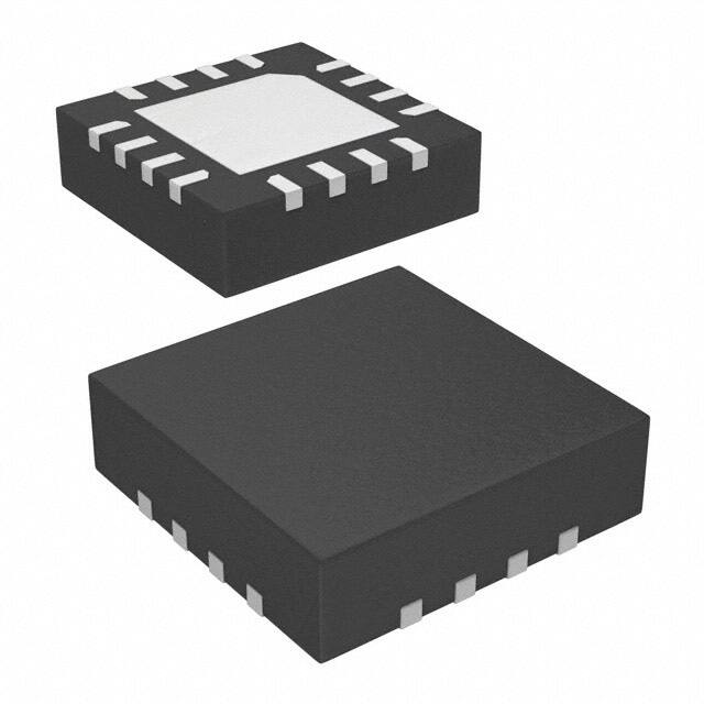
Available in 4 x 4 x 0.8 mm and 3 x 3 x 0.8 mm
16-pin TQFN packages
LED current is easily adjustable by an external
resistor up to 30 mA per channel.
The CTRL0, CTRL1, and CTRL2 logic inputs function
as a LED enable and a PWM mode LED brightness
control.
APPLICATION
o
o
Keypad and Display Backlight
Cellular Phones
o
o
Digital Still Cameras
PDAs and Smartphones
The driver supports a wide range of input voltages
from 2.7 V to 5.5 V.
The thermal and short circuit protection guarantee
high device reliability.
DESCRIPTION
The device is available in a 16-lead TQFN 4 x 4 mm
and 3 x 3 mm packages with a max height of 0.8 mm
.
The LDS8846 is a high efficiency ultra-low dropout
current regulator that can drive up to four LEDs. The
.
TYPICAL APPLICATION CIRCUIT
© 2009 IXYS Corp.
Characteristics subject to change without notice
1
Doc. No. 8845DS, Rev. N1.6
�LDS8846
ABSOLUTE MAXIMUM RATINGS
Parameter
V IN, LEDx voltage
V OUT voltage
EN, CTRL0, CTRL1, CTRL2 voltage
Storage Temperature Range
Junction Temperature Range
Soldering Temperature (10s)
ESD protection HBM
Rating
-0.3 to 6
-0.3 to 6
V IN + 0.7V
-65 to +150
-40 to +125
300
2
Unit
V
V
V
°C
°C
°C
kV
NOTE: Stresses listed above may cause permanent damage to thje device. Functional operation of the device at these or any other conditio ns
beyond those indicated in the “Recommended Operating Conditions” is not impiled. Exposure to abslute maximum rating conditions for
extended periods may remain possibility to affect device reliability.
RECOMMENDED OPERATING CONDITIONS
Parameter
Rating
2.7 to 5.5
-40 to +85
V IN
Ambient Temperature Range
Unit
V
°C
ELECTRICAL OPERATING CHARACTERISTICS
(Over recommended operating conditions unless specified otherwise) V IN = 3.6V, EN = High, TAMB = 25°C
Name
Conditions
Quiescent Current
Shutdown Current
LED Current
Typ
Max
Units
ILED = 20mA per channel
1.3
1.5
mA
EN = 0V
RSET = 24k
0.1
1
µA
RSET = 96k
2.7 < V IN < 5.5V
To set value
(ILED MAX - ILED MIN) / (ILED
MAX + I LED MIN)
LED Current Setting Range
LED Current Accuracy
LED Channel Matching
Min
20
5
2
-8
-5
Current Sink Dropout Voltage*
Short Circuit Output Current Limit
EN, CTRL0,
CTRL1,
CTRL2 pins
Leakage Current
High
Low
High
Low
V OUT = 0V
Input Voltage = V IN
Input Voltage = 0
Logic Level
Threshold
PWM frequency
PWM duty cycle
Thermal Shutdown
Thermal Hysteresis
Under Voltage Lockout (UVLO)
Threshold
*) Voltage
drop at led pin, at which LED current falls 10% below set value
© 2009 IXYS Corp.
Characteristics subject to change without notice
2
mA
3
30
+8
mA
%
3
+5
%
20
30
mV
22
25
1
mA
-1
1.3
0.4
100000
100
100
1
150
20
2.4
µA
V
Hz
%
°C
V
Doc. No. 8846DS, Rev. N1.6
�LDS8846
CONTROL INPUTS FUNCTION
Control Inputs
CTRL2
CTRL1 CTRL0
0
0
0
0
0
1
0
1
0
0
1
1
1
0
0
1
0
1
1
1
0
1
1
1
LED4
OFF
OFF
OFF
ON
OFF
OFF
ON
OFF
Output States
LED3 LED2
OFF
OFF
OFF
ON
ON
OFF
OFF
OFF
OFF
ON
ON
ON
ON
ON
OFF
OFF
LED1
ON
OFF
OFF
OFF
ON
ON
ON
OFF
TYPICAL CHARACTERISTICS
0
V IN = 3.6V, I OUT = 104 mA (4 LEDs at 26 mA each), CIN = COUT = 1 µF, Vf = 3.2 V, TAMB = 25 C
Power Efficiency vs. Input Voltage
LED Current vs. Temperature
LED Current vs. Input Voltage
Power-Up Delay Time
EN
V OUT
ILED
( 4 LEDs)
50 mA/div
© 2009 IXYS Corp.
Characteristics subject to change without notice
3
Doc. No. 8846DS, Rev. N1.6
�LDS8846
Power-Down Delay Time
PWM Mode (1 kHz, 50 Duty Cycle)
EN
CRL0
V OUT
V OUT
ILED
ILED
(4 LEDs)
(4 LEDs)
50 mA/div
50 mA/div
PWM Mode (10 kHz, 50 Duty Cycle)
PWM Mode (50 kHz, 50 Duty Cycle)
CRL0
CRL0
V OUT
VOUT
ILED
ILED
(4 LEDs)
(4 LEDs)
50 mA/div
50 mA/div
I LED Current vs. Duty Cycle
© 2009 IXYS Corp.
Characteristics subject to change without notice
ILED Current Error vs. Duty Cycle
4
Doc. No. 8846DS, Rev. N1.6
�LDS8846
PIN DESCRIPTION
Pin #
Name
1
2
3
4
5
6
7
8 - 11
12
13
14
15
16
PAD
EN
CTRL0
CTRL1
CTRL2
ISET
V OUT
VIN
NC
PGND
LED4
LED3
LED2
LED1
PAD
Function
Device Enable.
Output Control Bit 0 (See Table Control Pin Function)
Output Control Bit 1 (See Table Control Pin Function)
Output Control Bit 2 (See Table Control Pin Function)
LED current setting pin
Output voltage to the LED anodes
Input Voltage
No internal connect
Power Ground
LED4 Cathode Terminal
LED3 Cathode Terminal
LED2 Cathode Terminal
LED1 Cathode Terminal
Connect to GND on the PCB
PIN FUNCTION
supply falls below the under-voltage threshold (2.2
V), all the LED channels are disabled, and the device
enters shutdown mode.
EN is a Device Enable. This pin is high impedance.
There should be a pull down resistor
很抱歉,暂时无法提供与“LDS8846-002-T2”相匹配的价格&库存,您可以联系我们找货
免费人工找货