LDS8869
6-Channel Ultra Low Dropout LED Driver
FEATURES
o
Charge pump modes: 1x, 1.33x, 1.5x, 2x
Ultra low dropout PowerLite™ Current
Regulator*
Drives up to 6 LEDs at 32mA each
o
o
1-wire LED current programming
Power efficiency up to 94%
o
Low input noise & ripple in all charge pump
modes
o
o
Low current shutdown mode
Short circuit current limiting
o
Thermal shutdown protection
o
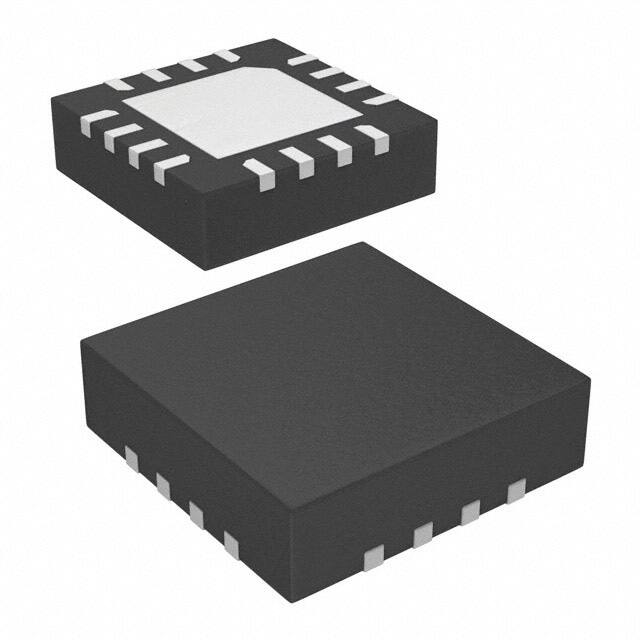
Available in 3 x 3 x 0.8 mm 16-pin TQFN
package
o
o
device’s efficiency up to 94%. New mode requires no
additional external capacitors.
The EN/SET logic input functions as a chip enable
and a current setting interface.
The LEDs current is programmable by one wire
digital interface from 0.5 to 32mA in 0.5mA steps or
from zero to 3.75mA in 0.25mA steps. Every LED
bank with two LEDs each may be turned on/off or
programmed separately
APPLICATION
o
Keypad and Display Backlight
o
o
Cellular Phones
Digital Still Cameras
o
PDAs and Smartphones
Low noise input ripple is achieved by operating at a
constant switching frequency which allows the use of
small external ceramic capacitors. The multifractional charge pump supports a wide range of
input voltages from 2.7V to 5.5V.
DESCRIPTION
The LDS8869 is a high efficiency multi-mode
fractional charge pump with ultra low dropout voltage
that can drive up to six LEDs. Inclusion of a 1.33x
fractional charge pump mode and ultra low dropout
PowerLite™ Current Regulator (PCR) increases
The device is available in in 16-lead TQFN 3 mm x 3
mm package with a max height of 0.8 mm.
TYPICAL APPLICATION CIRCUIT
© 2009 IXIS Corp.
Characteristics subject to change without notice
1
Doc. No. 8869_DS, Rev. N2.1
�LDS8869
ABSOLUTE MAXIMUM RATINGS
Parameter
V IN, LEDx, C1±, C2± voltage
V OUT voltage
EN/SET voltage
Storage Temperature Range
Junction Temperature Range
Soldering Temperature
Rating
6
6
V IN + 0.7V
-65 to +160
-40 to +125
300
Unit
V
V
V
°C
°C
°C
RECOMMENDED OPERATING CONDITIONS
Parameter
V IN
Ambient Temperature Range
Rating
2.7 to 5.5
-40 to +85
Unit
V
°C
Typical application circuit with external components is shown on page 1.
ELECTRICAL OPERATING CHARACTERISTICS
(Over recommended operating conditions unless specified otherwise) Vin = 3.6V, C1 = C2 = 0.22 µF, Cin = Cout = 1 µF, EN = High, TAMB =
25°C
Name
Quiescent Current
Shutdown Current
LED Current Accuracy
LED Channel Matching
Output Resistance (open loop)
Conditions
1x mode, no load
1
Charge Pump Frequency
Output short circuit Current Limit
Input Current Limit
1x to 1.33x, 1.33x to 1.5x, or 1.5x to 2x
Transition Thresholds at any LED pin
1.33x to 1x Mode Transition Hysteresis
Transition Filter Delay
Input Leakage
EN/SET
Pin
High
Logic Level
Low
Thermal Shutdown
Thermal Hysteresis
Under Voltage Lockout (UVLO)
Threshold
Over Voltage Protection
V EN = 0V
1mA ≤ILED ≤31mA
(ILED - ILEDAVG) / ILEDAVG
1x mode
1.33x mode
1.5x mode
2x mode
1.33x
1.5x mode and 2x mode
V OUT < 0.5V
Min
Typ
1.7
-5
-5
±3
±3
0.8
3.5
5.5
6.5
0.8
1.1
35
450
ILED = 30 mA
75
Max
2.5
1
+5
+5
Ω
MHz
mA
mA
130
mV
1
mV
µs
µA
600
800
-1
1.3
Units
mA
µA
%
%
0.4
150
20
2.2
V
°C
6.2
V
V
Note: 1. Sample test only
© 2009 IXIS Corp.
Characteristics subject to change without notice
2
Doc. No. 8869_DS, Rev. N2.1
�LDS8869
RECOMMENDED EN/SET TIMING
For 2.5 VIN 5.5V, over full ambient temperature range -40 to +85ºC.
Symbol
Name
Max
Units
tSETUP
tLO
EN/SET setup from shutdown
EN/SET program low time
Conditions
Min
10
0.2
Typ
100
100
μs
μs
tHI
tOFF
0.2
1.5
500
100
tDATADELAY
EN/SET program high time
EN/SET low time to shutdown
EN/SET Delay to DATA
μs
ms
μs
tRESETDELAY
EN/SET Delay High to ADDRESS
2
ms
Figure 1. EN/SET One Wire Addressable Timing Diagram
REGISTER CONFIGURATION AND PROGRAMMING
Table 1. Register Address and Data
Register
REG1
REG2
REG3
REG4
REG5
REG6
Address
Pulses
1
2
3
4
5
6
Description
Bits
Bank Enable and IMODE
Global Current Setting*
Bank C Current Setting
Bank B Current Setting
Bank A Current Setting
Return Lockout
4
6
6
6
6
1
Bit 3
IMODE
DATA pattern
Bit 2
Bit 1
ENC
ENB
Bit 0
ENA
See Table 3 for values
RTLKO
Note: *) If Global current setting register Reg2 is used, registers Reg3 – Reg5 should be empty, and vice versa If registers Reg3 – Reg5 are
used, Reg2 should be empty to prevent data interference.
Table 2. Reg1 Code
Data
pulses
0
1
2
3
4
5
3
0
1
1
1
1
1
Reg1 Bit
2 1
0 0
1 1
1 1
1 0
1 0
0 1
0
0
1
0
1
0
1
Data
pulses
6
7
8
9
10
11
3
1
1
1
0
0
0
Reg1 Bit
2 1
0 1
0 0
0 0
1 1
1 1
1 0
0
0
1
0
1
0
1
Data
pulses
12
13
14
15
16
3
0
0
0
0
0
Reg1 Bit
2 1
1 0
0 1
0 1
0 0
0 0
0
0
1
0
1
0
Note: If bits Bit0 – Bit2 are set to zero, the corresponding LED bank is disabled.
© 2009 IXIS Corp.
Characteristics subject to change without notice
3
Doc. No. 8869_DS, Rev. N2.1
�LDS8869
Table 3. REG2-5 Current Setting Registers
Data
Pulses
0
1
2
3
4
5
6
7
8
9
10
11
12
13
14
15
16
17
18
19
20
21
22
23
24
25
26
27
28
29
30
31
32
Reg2-5 value
(binary)
000000
111111
111110
111101
111100
111011
111010
111001
111000
110111
110110
110101
110100
110011
110010
110001
110000
101111
101110
101101
101100
101011
101010
101001
101000
100111
100110
100101
100100
100011
100010
100001
100000
LED Current,
mA, IMODE = 0
0.0
3.75
3.5
3.25
3
2.75
2.5
2.25
2
1.75
1.5
1.25
1
0.75
0.5
0.25
0.0
© 2009 IXIS Corp.
Characteristics subject to change without notice
LED Current,
mA, IMODE = 1
0.5
32
31.5
31.0
30.5
30
29.5
29
28.5
28
27.5
27
26.5
26
25.5
25
24.5
24
23.5
23
22.5
22
21.5
21
20.5
20
19.5
19
18.5
18
17.5
17
16.5
Data
Pulses
33
34
35
36
37
38
39
40
41
42
43
44
45
46
47
48
49
50
51
52
53
54
55
56
57
58
59
60
61
62
63
64
4
Reg2-5 value
(binary)
011111
011110
011101
011100
011011
011010
011001
011000
010111
010110
010101
010100
010011
010010
010001
010000
001111
001110
001101
001100
001011
001010
001001
001000
000111
000110
000101
000100
000011
000010
000001
000000
LED Current,
mA, IMODE = 0
LED Current,
mA, IMODE = 1
16
15.5
15
14.5
14
13.5
13
12.5
12
11.5
11
10.5
10
9.5
9
8.5
8
7.5
7
6.6
6
5.5
5
4.5
4
3.5
3
2.5
2
1.5
1
0.5
Doc. No. 8869_DS, Rev. N2.1
�LDS8869
PROGRAMMING EXAMPLES
Programming 6 LEDs to 32mA
Programming 6 LED to 1mA
© 2009 IXIS Corp.
Characteristics subject to change without notice
5
Doc. No. 8869_DS, Rev. N2.1
�LDS8869
TYPICAL CHARACTERISTICS
Vin = 3.6V, IOUT = 120mA (6 LEDs at 20mA), C 1 = C2 = 0.22 μF, CIN = C OUT = 1μ
F, T AMB = 25°C unless otherwise specified
Efficiency vs. Input Voltage
Power-Up in 1x Mode
EN/SET
VOUT
ILED
100mA/div
Power-Up in 1.33x Mode
Power-Up in 1.5x Mode
EN/SET
EN/SET
V OUT
V OUT
ILED
100mA/div
ILED
100mA/div
Power-Up in 2x Mode
Power-Down Delay (1x Mode)
EN/SET
EN/SET
VOUT
VOUT
ILED
100mA/div
ILED
100mA/div
© 2009 IXIS Corp.
Characteristics subject to change without notice
6
Doc. No. 8869_DS, Rev. N2.1
�LDS8869
Operating Waveforms in 1x Mode
Operating Waveforms in 1.33x Mode
VIN
VIN
V OUT
VOUT
ILED
100mA/div
ILED
100mA/div
Operating Waveforms in 1.5x Mode
Operating Waveforms in 2x Mode
V IN
V IN
V OUT
V OUT
ILED
100mA/div
© 2009 IXIS Corp.
Characteristics subject to change without notice
ILED
100mA/div
7
Doc. No. 8869_DS, Rev. N2.1
�LDS8869
PIN DESCRIPTION
Pin #
1
2
3
4
5
6
7
8
9
10
11
12
13, 14
15
16
TAB
Name
LEDC2
LEDC1
LEDB2
LEDB1
LEDA2
LEDA1
VOUT
V IN
C1+
C1C2+
C2GND
GND
EN/SET
TAB
Function
LEDC2 cathode terminal
LEDC1 cathode terminal
LEDB2 cathode terminal
LEDB1 cathode terminal
LEDA2 cathode terminal
LEDA1 cathode terminal
Charge pump output connected to the LED anodes
Charge pump input, connect to battery or supply
Bucket capacitor 1 Positive terminal
Bucket capacitor 1 Negative terminal
Bucket capacitor 2 Positive terminal
Bucket capacitor 2 Negative terminal
Ground Reference
Ground Reference
Device enable (active high) and Dimming Control
Connect to GND on the PCB
Top view: TQFN 16-lead 3 X 3 mm
PIN FUNCTION
capacitor is required between the Vout pin and
ground near the device.
VIN is the supply pin for the charge pump. A small 1μF
ceramic bypass capacitor is required between the Vin
pin and ground near the device. The operating input
voltage range is from 2.5V to 5.5V. Whenever the
input supply falls below the under-voltage threshold
(2.2 V), all the LED channels are disabled and the
device enters shutdown mode.
GND is the ground reference for the charge pump.
The pin must be connected to the ground plane on
the PCB.
C1+, C1- are connected to each side of the ceramic
bucket capacitor C1
EN/SET is the enable and one wire addressable
control logic input for all LED channels. Guaranteed
levels of logic high and logic low are set at 1.3V and
0.4V respectively. When EN/SET is initially taken
high, the device becomes enabled and all LED
currents remain at 0mA. To place the device into zero
current mode, the EN/SET pin must be held low for
more than 1.5ms.
C2+, C2- are connected to each side of the ceramic
bucket capacitor C2
LEDA1 – LEDC2 provide the internal regulated
current source for each of the LED cathodes. These
pins enter high-impedance zero current state
whenever the device is in shutdown mode.
TAB is the exposed pad underneath the package.
For best thermal performance, the tab should be
soldered to the PCB and connected to the ground
plane
VOUT is the charge pump output that is connected to
the LED anodes. A small 1μF ceramic bypass
© 2009 IXIS Corp.
Characteristics subject to change without notice
8
Doc. No. 8869_DS, Rev. N2.1
�LDS8869
BLOCK DIAGRAM
Figure 2. LDS8869 Functional Block Diagram
BASIC OPERATION
At power-up, EN pin should be logic LOW. During
power-up device performs internal circuits reset that
requires less than 10µs. To start device, EN pin
should be set logic HIGH at least 10µs after V IN
applied. Device starts operating at 1x mode at which
the V OUT is approximately equal to VIN (less any
internal voltage losses). If the output voltage is
sufficient to regulate all LED currents, the device
remains in 1x operating mode.
Regulator switches the charge pump into 1.33x mode
(after a fixed delay time of about 800μs). In 1.33x
mode, the charge pump’ output voltage is
approximately equal to 1.33 times the input supply
voltage (less any internal voltage losses).
This sequence repeats at every mode until driver
enters the 2x mode.
If the device detects a sufficient input voltage is
present to drive all LED currents in 1x mode, it will
change automatically back to 1x mode. This only
applies for changing back to the 1x mode. The
difference between the input voltage when exiting 1x
mode and returning to 1x mode is called the 1x mode
transition hysteresis (about 600mV).
. The low dropout PowerLite™ Current regulator
(PCR) performs well at input voltages up to 75 mV
above LED forward voltage V F significantly increasing
driver’s efficiency. The LDS8869 monitors voltage
drop Vd across PCR at every channel in ON state. If
this voltage falls below 75 mV (typical) at any one
channel, (channel with LED with highest forward
voltage), the Mode Control Block changes charge
pump mode to the next multiplication ratio.
LED Current Setting
The current in each of the six LED channels is
programmed through the 1-wire EN/SET digital
control input. By pulsing this signal according to a
specific protocol, a set of internal registers can be
addressed and written into allowing to configure each
bank of LEDs with the desired current. There are six
registers: the first five are 4 bits long and the sixth is
1 bit long. The registers are programmed by first
Vd (LEDX1/2) = V IN x M – V F – Rcp x Iout, where Rcp
is a Charge Pump Output Resistance at given mode,
Iout is sum of all LED currents, and M is a charge
pump’ multiplication ratio.
If the input voltage is insufficient or falls to a level
where Vd ≤75 mV, and the regulated currents cannot
be maintained, the low dropout PowerLite™ Current
© 2009 IXIS Corp.
Characteristics subject to change without notice
9
Doc. No. 8869_DS, Rev. N2.1
�LDS8869
selecting the register address and then programming
data into that register.
REG6 contains the return lockout (RTLKO) bit. This
stops the charge pump returning to 1x mode. One
pulse sets it to 1. Two pulses set RTLKO to 0. When
RTLKO is set to 1, the charge pump cannot
automatically return to 1x mode when in one of the
charge pump modes. The device can however move
from 1x to 1.33x, or to 1.5x and 2x if the input voltage
is not sufficient to drive the programmed LED
currents.
An internal counter records the number of falling
edges to identify the address and data. The address
is serially programmed adhering to low and high
duration time delays. One down pulse corresponds to
register 1 being selected. Two down pulses
correspond to register 2 being selected and so on up
to register 6. tLO and tHI must be within 200ns to
100μs. Any pulse with less than 200 ns width may be
ignored.
REG6 also triggers a charge pump. This forces the
charge pump to start from 1x mode and determine
the correct mode it should be in to drive the LEDs
most efficiently. If the input voltage has risen or the
device has been reprogrammed to other LED values,
it is recommended to trigger this reset allowing the
charge pump to run in the most efficient mode.
Once the final rising edge of the address pulse is
programmed, the user must wait at least 500μs
before programming the first data pulse. Any falling
edge after this minimum delay will be recognised as a
first data pulse.
To power-down the device and turn-off all current
sources, the EN/SET input should be low for at least
1.5ms (tOFF) or longer. The driver typically powersdown with a delay of about 1ms. All register data are
cleared.
Data in a register is reset once it is selected by the
address pulses. If a register is selected but no data is
programmed, next pulse sequence will be recognized
as data only. Do not send register address only
without following data because it may disrupt normal
device operation.
Unused LED Channels
For applications with only four or two LEDs, unused
LED banks can be disabled via the enable register
internally and left to float or connect to Vout.
Once the final rising edge of the data pulses is
programmed, the user must wait at least 1.5ms
before
programming
another
address.
If
programming fails or is interrupted, the user must
wait at least 2 ms (tRESETDELAY) from the last rising
edge before reprogramming can commence.
For applications requiring 1, 3, or 5 channels, the
unused LED pins should be tied to V OUT (see Figure
3). If LED pin voltage is within 1 V of VOUT , then the
channel is switched off and a 250 μA test current is
placed in the channel to sense when the channel
moves below VOUT – 1.5 V.
Upon EN/SET pin goes high the device automatically
starts looking for an address. If no falling edge is
detected within 100μs, then the user must wait at
least 2 ms before trying to program the device again.
Protection Modes
The device requires a minimum 10μs delay to ensure
the initialization of the internal logic at power-up. After
this time delay, EN/SET pin may be set high and the
device registers may be programmed adhering to the
timing constraints shown in Figure 1.
The LDS8869 has follow protection modes:
Register REG1 allows to set the mode and select the
pairs of LEDs to be turned on. A low LED current
mode exists to allow for very low current operation
under 4mA per channel. If IMODE equals 1, the high
current range is selected up to 32mA. If IMODE is set
to 0, all currents are divided by 8. Each bank of LEDs
(A, B or C) can be turned on independently by setting
the respective bit ENA, ENB, ENC to 1.
Figure 3. Application circuit with 5 LEDs
Register REG2 allows to set the same current for all
6 channels. REG3, REG4, REG5 allow to set the
current respectively in banks C, B and A. The three
banks can be programmed with independent current
values.
© 2009 IXIS Corp.
Characteristics subject to change without notice
1. LED short to V OUT protection
If LED pin is shorted to V OUT , LED burned out
becomes as short circuit, or LED pin voltage is within
from V OUT to (VOUT - 1.5V) range, LDS8869
10
Doc. No. 8869_DS, Rev. N2.1
�LDS8869
recognizes this condition as “LED Short” and disables
this channel. If LED pin voltage is less than (Vout –
1.5V), LDS8869 restores LED current at this
particular channel to programmed value.
modes, the input current ripple is very low, and an
input bypass capacitor of 1µF is sufficient.
In 1x mode, the device operates in linear mode and
does not introduce switching noise back onto the
supply.
2. V OUT Over-Voltage Protection
The charge pump’ output voltage V OUT automatically
limits at about 6.2 V maximum. This is to prevent the
output pin from exceeding its absolute maximum
rating.
Recommended Layout
In charge pump mode, the driver switches internally
at a high frequency. It is recommended to minimize
trace length to all four capacitors. A ground plane
should cover the area under the driver IC as well as
the bypass capacitors. Short connection to ground on
capacitors CIN and COUT can be implemented with the
use of multiple via. A copper area matching the
TQFN exposed pad (TAB) must be connected to the
ground plane underneath. The use of multiple via
improves the package heat dissipation.
3. V OUT Short Circuit Protection
If VOUT is shorted to ground before LDS8869 is
enabled, input current may increase up to 200 – 300
mA within 20 µs after enable and is limited to 35 – 40
mA after that.
4. Over-Temperature Protection
If the die temperature exceeds +150°C, the driver will
enter shutdown mode. The LDS8869 requires restart
after die temperature falls below 130°C.
5. Input Voltage Under-Voltage Lockout
If V IN falls below 2.2 V (typical value), LDS8869
enters shutdown mode and all registers data are
cleared. Device requires restart when input voltage
rises above 2.3 V. To restart device, set EN/SET pin
logic low, turn VIN off/on, set EN/SET pin logic high,
and program ILED using 1-wire interface.
6. Low V IN or High LED VF Voltage Detection
If, in 2x mode, V IN is too low to maintain regulated
LED current for given LED VF, or LED becomes an
open circuit, or if any LED at active channels is
disconnected,
LDS8869
starts
subsequently
changing modes (2x – 1x – 1.33x -1.5x – 2x -…) in
an attempt to compensate insufficient voltage. As a
result, average current at all other channels that are
ON may fall below regulated level.
Figure 4. Recommended layout
LED Selection
LEDs with forward voltages (VF ) ranging from 1.6 V to
3.6 V may be used. Charge pumps operate in highest
efficiency when V F voltage is close to VIN voltage
multiplied by switching mode, i.e. V IN x 1, VIN x 1.33,
and so on. If the power source is a Li-ion battery,
LEDs with VF = 2.7V - 3.3V are recommended to
achieve highest efficiency performance and extended
operation on a single battery charge.
External Components
The driver requires two external 1 µF ceramic capacitors (CIN and C OUT) and two 0.22 µF ceramic capacitors (C1 and C2) X5R or X7R type. Capacitors C1
and C2 may be increased up to 1 µF to improve
charge pump efficiency by 3%. In all charge pump
© 2009 IXIS Corp.
Characteristics subject to change without notice
11
Doc. No. 8869_DS, Rev. N2.1
�LDS8869
PACKAGE DRAWING AND DIMENSIONS
16-PIN TQFN (HV3), 3mm x 3mm, 0.5mm PITCH
SYMBOL
A
A1
A2
b
D
D1
E
E1
e
L
m
n
MIN
0.70
0.00
0.178
0.20
2.95
1.65
2.95
1.65
0.325
NOM
0.75
0.02
0.203
0.25
3.00
1.70
3.00
1.70
0.50 typ
0.375
0.150 typ
0.225 typ
MAX
0.80
0.05
0.228
0.30
3.05
1.75
3.05
1.75
0.425
Note:
1. All dimensions are in millimeters
2. Complies with JEDEC Standard MO-220
© 2009 IXIS Corp.
Characteristics subject to change without notice
12
Doc. No. 8869_DS, Rev. N2.1
�LDS8869
ORDERING INFORMATION
Part Number
LDS8869 002-T2
Notes:
1.
2.
Package
Package Marking
(1)
TQFN-16 3 x 3mm
8869
Matte-Tin Plated Finish (RoHS-compliant)
Quantity per reel is 2000
EXAMPLE OF ORDERING INFORMATION
Prefix
LDS
Device #
Suffix
8869
002
Product Number
Optional
Company ID
Package
T2
Tape & Reel
T: Tape & Reel
2: 2000/Reel
002: 3x3 TQFN
Notes:
1) All packages are RoHS-compliant (Lead-free, Halogen-free).
2) The standard lead finish is Matte-Tin.
3) The device used in the above example is a LDS8869 002–T2 ( 3x3 TQFN, Tape & Reel).
4) For additional package and temperature options, please contact your nearest IXIS Corp. Sales office.
© 2009 IXIS Corp.
Characteristics subject to change without notice
13
Doc. No. 8869_DS, Rev. N2.1
�LDS8869
Warranty and Use
IXIS CORP. MAKES NO WARRANTY, REPRESENTATION OR GUARANTEE, EXPRESS OR IMPLIED, REGARDING THE SUITABILITY OF ITS PRODUCTS FOR ANY
PARTICULAR PURPOSE, NOR THAT THE USE OF ITS PRODUCTS WILL NOT INFRINGE ITS INTELLECTUAL PROPERTY RIGHTS OR THE RIGHTS OF THIRD
PARTIES WITH RESPECT TO ANY PARTICULAR USE OR APPLICATION AND SPECIFICALLY DISCLAIMS ANY AND ALL LIABILITY ARISING OUT OF ANY SUCH
USE OR APPLICATION, INCLUDING BUT NOT LIMITED TO, CONSEQUENTIAL OR INCIDENTAL DAMAGES.
IXIS Corp. products are not designed, intended, or authorized for use as components in systems intended for surgical implant into the body, or other applications intended to
support or sustain life, or for any other application in which the failure of the IXIS Corp. product could create a situation where personal injury or death may occur.
IXIS Corp. reserves the right to make changes to or discontinue any product or service described herein without notice. Products with data sheets labeled "Advance
Information" or "Preliminary" and other products described herein may not be in production or offered for sale.
IXIS Corp. advises customers to obtain the current version of the relevant product information before placing orders. Circuit diagrams illustrate typical semiconductor
applications and may not be complete.
IXIS Corp.
1590 Buckeye Dr.,
Milpitas, CA 95035-7418
Phone: 408.457.9000
Fax:
408.496.0222
http://www.ixys.com
© 2009 IXIS Corp.
Characteristics subject to change without notice
Document No: 8869_DS
Revision:
N2.1
Issue date:
10/7/2009
14
Doc. No. 8869_DS, Rev. N2.1
�