LKK 47-06C5
Advanced Technical Information
Dual CoolMOS™ 1) Power MOSFET
VDSS
= 600 V
ID25
= 47 A
Ω/MOSFET
RDS(on) max = 45 mΩ
Common Source Topology
DCB isoated package
4
D1
T1
2
G1
3
S
1
2
3
4
5
T2
1
G2
5
D2
Features
MOSFET T1/T2
Symbol
Conditions
VDSS
VD1D2
TVJ = 25°C
TVJ = 25°C
Maximum Ratings
VGS
600
±600
V
V
±20
V
47
32
A
A
1950
3
mJ
mJ
ID25
ID90
TC = 25°C
TC = 90°C
EAS
EAR
single pulse
repetitive
Symbol
Conditions
RDSon
VGS = 10 V; ID = 44 A
40
45 mΩ
RDSon
total between D1 and D2
VG1S = VG2S = 10 V; ID = 44 A
80
mΩ
VGSth
VDS = VGS; ID = 3 mA
IDSS
VDS = VDSS; VGS = 0 V; TVJ = 25°C
TVJ = 125°C
ID = 11 A; TC = 25°C
Characteristic Values
(TVJ = 25°C, unless otherwise specified)
min.
typ. max.
2.5
3
3.5
V
10
µA
µA
100
nA
50
IGSS
VGS = ±20 V; VDS = 0 V
Ciss
Coss
VGS = 0 V; VDS = 100 V
f = 1 MHz
Qg
Qgs
Qgd
VGS= 0 to10 V; VDS = 400 V; ID = 44 A
150
35
50
td(on)
tr
td(off)
tf
VGS= 10 V; VDS = 400 V;
ID = 44 A; RG = 3.3 Ω
30
20
100
10
ns
ns
ns
ns
RthJC
RthCH
with heatsink compound
0.25
0.45 K/W
K/W
IXYS reserves the right to change limits, test conditions and dimensions.
© 2009 IXYS All rights reserved
6800
320
• fast CoolMOS™ 1) power MOSFET
4th generation
- High blocking capability
- Lowest resistance
- Avalanche rated for unclamped
inductive switching (UIS)
- Low thermal resistance
due to reduced chip thickness
• Enhanced total power density
Applications
• AC Switch
- power regulation of AC heating
- light dimming
• Power factor correction (PFC)
interleaved operation mode
• Push pull converter
1)
CoolMOS™ is a trademark of
Infineon Technologies AG.
pF
pF
190
nC
nC
nC
20090209b
1-4
�Advanced Technical Information
LKK 47-06C5
Source-Drain Diode
Characteristic Values
(TJ = 25°C, unless otherwise specified)
min.
typ. max.
IS
VGS = 0 V
VSD
IF = 44 A; VGS = 0 V
t rr
QRM
IRM
IF = 44 A; -di/dt = 100 A/µs; VR = 400 V
0.9
44
A
1.2
V
600
17
60
ns
µC
A
Component
Symbol
Conditions
Maximum Ratings
TVJ
Tstg
VISOL
IISOL < 1 mA; 50/60 Hz; t = 1 min
FC
Mounting force with clip
Symbol
Conditions
CP
coupling capacity between shorted
pins and mounting tab in the case
dS, dA
dS, dA
pin - pin
pin - backside metal
Weight
-55...+150
-55...+150
°C
°C
2500
V~
40 - 180
N
Characteristic Values
min.
typ. max.
50
tbd
tbd
pF
mm
mm
10
g
20090209b
© 2009 IXYS All rights reserved
2-4
�LKK 47-06C5
Advanced Technical Information
ISOPLUS264
S
U
A
E
R1
D
Q1
T
R
Q
A2
6
1
3
4
5
L
L1
2
b
c
b2
b1
b3
A1
e
NOTE:
1.TAP 6 = ELECTRICALLY ISOLATED 2,500V FROM THEOTHERPINS.
2. ALL LEADSAREPb FREESOLDER DIPPE
D.
All curves for single MOSFET T1 or T2 only
250
TJ = 25°C
VGS = 20 V
140
10 V 8 V
8V
TJ = 150°C
7V
10 V
120
7V
200
6V
VGS = 20 V
100
5.5 V
150
I D [A]
I D [A]
80
6V
60
100
5V
5.5 V
40
4.5 V
5V
50
20
4.5 V
0
0
0
5
10
15
20
0
5
10
15
20
V DS [V]
V DS [V]
Fig. 1 Typ. output characteristics
Fig. 2 Typ. output characteristics
20090209b
© 2009 IXYS All rights reserved
3-4
�LKK 47-06C5
Advanced Technical Information
0.16
320
0.12
ID = 44 A
VGS = 10 V
TJV = 150°C
5.5 V
VDS = 5 V
6V
6.5 V
7V
0.12
VDS > 2·RDS(on) max · ID
25 °C
280
0.1
240
0.08
0.08
I D [A]
R DS(on) [ ]
R DS(on) [ ]
200
20 V
0.06
98 %
160
150 °C
120
typ
TJ =
0.04
0.04
80
0.02
40
0
0
0
20
40
60
80
0
100
-60
-20
20
60
I D [A]
140
180
0
2
4
T j [°C]
Fig. 3 Typ. drain-source on-state
resistance
10
100
Fig. 4 Drain-source on-state
resistance
3
6
8
10
V GS [V]
Fig. 5 Typ. transfer characteristics
12
10
5
ID = 11 A pulsed
VGS = 0 V
f = 1 MHz
10
10
4
10
3
Ciss
VDS = 50 V
2
1 20 V
8
150 °C, 98%
25 °C
40 0V
I F [A]
V GS [ V]
TJ = 150 °C
C [ p F]
10
6
25 °C, 98%
10
1
Coss
10
2
10
1
10
0
4
Crss
2
10
0
0
0
0.5
1
1.5
2
0
50
100
0
150
Fig. 6 Forward characteristic
of reverse diode
100
200
Fig. 8 Typ. capacitances
700
10
ID = 11 A
150
V DS [V]
Fig. 7 Typ. gate charge
2000
0
ID = 0.25 mA
1500
660
0.5
1000
-1
Z th J C [ K / W ]
V BR(DSS) [ V]
10
E AS [ m J ]
50
Q gate [nC]
V SD [V]
620
0.2
D = tp/T
0.1
0.05
10
-2
0.02
500
580
0.01
0
540
20
60
100
140
T j [°C]
Fig. 9 Avalanche energy
180
10
-60
-20
20
60
100
140
T j [°C]
180
single pulse
-3
10
-6
10
-5
10
-4
10
-3
10
-2
10
-1
10
0
t p [s]
Fig. 10 Drain-source breakdown voltage
20090209b
© 2009 IXYS All rights reserved
4-4
�Disclaimer Notice - Information furnished is believed to be accurate and reliable. However, users should independently
evaluate the suitability of and test each product selected for their own applications. Littelfuse products are not designed for,
and may not be used in, all applications.Read complete Disclaimer Notice at www.littelfuse.com/disclaimer-electronics.
�
很抱歉,暂时无法提供与“LKK47-06C5”相匹配的价格&库存,您可以联系我们找货
免费人工找货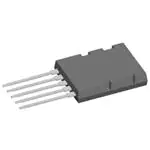


 工商网监
湘ICP备2023018690号
工商网监
湘ICP备2023018690号
