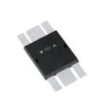
DE375-102N15A
RF Power MOSFET
N-Channel Enhancement Mode
Low Qg and Rg
High dv/dt
Nanosecond Switching
50MHz Maximum Frequency
Symbol
Test Conditions
Maximum Ratings
VDSS
TJ = 25°C to 150°C
1000
V
VDGR
TJ = 25°C to 150°C; RGS = 1 MΩ
1000
V
VGS
Continuous
±20
V
VGSM
Transient
±30
V
ID25
Tc = 25°C
15
A
IDM
Tc = 25°C, pulse width limited by TJM
90
A
IAR
Tc = 25°C
15
A
EAR
Tc = 25°C
1
J
5
V/ns
dv/dt
IS ≤ IDM, di/dt ≤ 100A/µs, VDD ≤ VDSS,
Tj ≤ 150°C, RG = 0.2Ω
>200
V/ns
940
W
425
W
4.5
W
IS = 0
PDC
PDHS
Tc = 25°C
Derate 3.7W/°C above 25°C
PDAMB
Tc = 25°C
Symbol
Test Conditions
min.
VDSS
VGS = 0 V, ID = 3 ma
1000
VGS(th)
VDS = VGS, ID = 1 ma
4.0
IGSS
VGS = ±20 VDC, VDS = 0
IDSS
VDS = 0.8 VDSS TJ = 25°C
VGS = 0
TJ = 125°C
RDS(on)
VGS = 15 V, ID = 0.5ID25
Pulse test, t ≤ 300µS, duty cycle d ≤ 2%
RthJC
RthJHS
VDS = 15 V, ID = 0.5ID25, pulse test
Weight
V
5.4
-55
=
15 A
RDS(on)
≤
1.0 Ω
PDC
=
940 W
GATE
SG2
SD1
SD2
-55
• Isolated Substrate
-High isolation voltage (>2500V)
-Excellent thermal transfer
6.0
V
±100
nA
-Increased temperature and power
cycling capability
50
1
µA
mA
• IXYS advanced low Qg process
• Low gate charge and capacitances
1.00
Ω
-Easier to drive
0.13 °C/W
°C/W
13.0
S
+150
°C
150
1.6mm (0.063 in) from case for 10 s
ID25
Features
max.
11.3
TJM
TL
typ.
0.3
Tstg
1000 V
Characteristic Values
TJ = 25°C unless otherwise specified
TJ
=
DRAIN
SG1
gfs
VDSS
°C
+150
°C
300
°C
3
g
-Faster switching
• Low RDS(on)
• Very low insertion inductance (
很抱歉,暂时无法提供与“375-102N15A-00”相匹配的价格&库存,您可以联系我们找货
免费人工找货