CLA40E1200NPZ
High Efficiency Thyristor
VRRM
=
1200 V
I TAV
=
40 A
VT
=
1.26 V
Two Quadrants Operation QI & QII
Single Thyristor with two gate polarities
Part number
CLA40E1200NPZ
Marking on Product: CLA40E1200NPZ
Backside: anode
Two Quadrants Operation
Positive Half Cycle
+
T2
(-)
T2
(+)
T1
2/4
T1
REF
1
REF
IGT -
+ IGT
± IGT
3
-
Negative Half Cycle
Note: All Polarities are referenced to T1
Features / Advantages:
Applications:
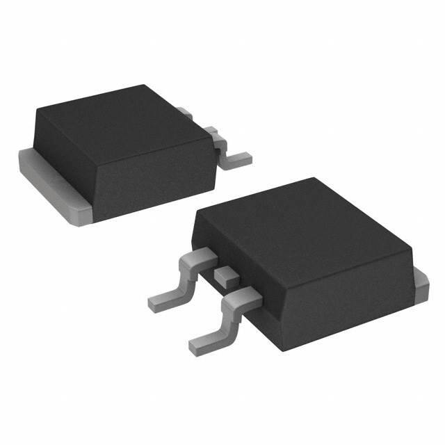
Package: TO-263 (D2Pak-HV)
● Thyristor for line frequency
● Planar passivated chip
● Long-term stability
● Two gate current polarities usable
- positive -> quadrant I
- negative -> quadrant II
● Thyristor can be used as Triac
- anti-parallel combination with AGT
- Anode-Gated-Thyristor covers quadrant III
- AGT-counterpart: CLB40I1200PZ
● Line rectifying 50/60 Hz
● Softstart AC motor control
● DC Motor control
● Power converter
● AC power control
● Lighting and temperature control
● Industry standard outline
● RoHS compliant
● Epoxy meets UL 94V-0
Disclaimer Notice
Information furnished is believed to be accurate and reliable. However, users should independently
evaluate the suitability of and test each product selected for their own applications. Littelfuse products are not designed for,
and may not be used in, all applications. Read complete Disclaimer Notice at www.littelfuse.com/disclaimer-electronics.
IXYS reserves the right to change limits, conditions and dimensions.
© 2019 IXYS all rights reserved
Data according to IEC 60747and per semiconductor unless otherwise specified
20190212c
�CLA40E1200NPZ
Ratings
Thyristor
Conditions
Symbol
VRSM/DSM
Definition
max. non-repetitive reverse/forward blocking voltage
TVJ = 25°C
VRRM/DRM
max. repetitive reverse/forward blocking voltage
TVJ = 25°C
1200
I R/D
reverse current, drain current
VT
forward voltage drop
TVJ = 25°C
10
µA
2
mA
TVJ = 25°C
1.30
V
1.59
V
1.26
V
IT =
40 A
IT =
80 A
IT =
40 A
IT =
80 A
I T(RMS)
RMS forward current
180° sine
VT0
threshold voltage
rT
slope resistance
R thJC
thermal resistance junction to case
TVJ = 125 °C
for power loss calculation only
thermal resistance case to heatsink
total power dissipation
I TSM
max. forward surge current
value for fusing
V
TVJ = 125°C
TC = 125 °C
RthCH
max. Unit
1300
V
VR/D = 1200 V
average forward current
Ptot
typ.
VR/D = 1200 V
I TAV
I²t
min.
1.64
V
T VJ = 150 °C
40
A
63
A
TVJ = 150 °C
0.85
V
9.9
mΩ
0.4 K/W
0.25
K/W
TC = 25°C
310
W
t = 10 ms; (50 Hz), sine
TVJ = 45°C
520
A
t = 8,3 ms; (60 Hz), sine
VR = 0 V
560
A
t = 10 ms; (50 Hz), sine
TVJ = 150 °C
440
A
t = 8,3 ms; (60 Hz), sine
VR = 0 V
475
A
t = 10 ms; (50 Hz), sine
TVJ = 45°C
1.35 kA²s
t = 8,3 ms; (60 Hz), sine
VR = 0 V
1.31 kA²s
t = 10 ms; (50 Hz), sine
TVJ = 150 °C
970
A²s
940
A²s
t = 8,3 ms; (60 Hz), sine
VR = 0 V
CJ
junction capacitance
VR = 400 V f = 1 MHz
TVJ = 25°C
PGM
max. gate power dissipation
t P = 30 µs
T C = 150 °C
19
t P = 300 µs
PGAV
average gate power dissipation
(di/dt) cr
critical rate of rise of current
TVJ = 150 °C; f = 50 Hz
repetitive, IT = 120 A
t P = 200 µs; di G /dt = 0.3 A/µs;
(dv/dt)cr
critical rate of rise of voltage
V = ⅔ VDRM
VGT
gate trigger voltage
I GT
gate trigger current
VGD
gate non-trigger voltage
I GD
gate non-trigger current
IL
latching current
IG =
0.3 A; V = ⅔ VDRM
non-repet., I T =
pF
10
W
5
W
0.5
W
150 A/µs
40 A
500 A/µs
TVJ = 150°C
500 V/µs
VD = 6 V
TVJ = 25 °C
1.7
TVJ = -40 °C
1.9
V
VD = 6 V
TVJ = 25 °C
± 35
mA
TVJ = -40 °C
± 55
mA
TVJ = 150°C
0.2
V
±1
mA
TVJ = 25 °C
100
mA
R GK = ∞; method 1 (linear voltage rise)
VD = ⅔ VDRM
tp =
10 µs
IG =
0.3 A; di G /dt =
V
0.3 A/µs
IH
holding current
VD = 6 V R GK = ∞
TVJ = 25 °C
70
mA
t gd
gate controlled delay time
VD = ½ VDRM
TVJ = 25 °C
2
µs
tq
turn-off time
IG =
0.3 A; di G /dt =
VR = 100 V; I T =
0.3 A/µs
40A; V = ⅔ VDRM TVJ =125 °C
di/dt = 10 A/µs dv/dt =
IXYS reserves the right to change limits, conditions and dimensions.
© 2019 IXYS all rights reserved
150
µs
20 V/µs t p = 200 µs
Data according to IEC 60747and per semiconductor unless otherwise specified
20190212c
�CLA40E1200NPZ
Package
Ratings
TO-263 (D2Pak-HV)
Symbol
I RMS
Definition
Conditions
RMS current
per terminal
min.
TVJ
virtual junction temperature
T op
operation temperature
Tstg
storage temperature
-40
typ.
max.
35
Unit
A
-40
150
°C
-40
125
°C
150
°C
1.5
Weight
FC
20
mounting force with clip
d Spp/App
Product Marking
C
L
A
40
E
1200
N
PZ
IXYS yywwZ
Logo
Date Code
Location
N
4.2
mm
terminal to backside
4.7
mm
Part description
XXXXXXXXX
Part Number
60
terminal to terminal
creepage distance on surface | striking distance through air
d Spb/Apb
g
123456
=
=
=
=
=
=
=
=
Thyristor (SCR)
High Efficiency Thyristor
(up to 1200V)
Current Rating [A]
Single Thyristor with two gate polarities
Reverse Voltage [V]
Three Quadrants operation: QI - QIII
TO-263AB (D2Pak) (2HV)
Lot#
Ordering
Standard
Alternative
Ordering Number
CLA40E1200NPZ-TRL
CLA40E1200NPZ-TUB
Equivalent Circuits for Simulation
I
V0
R0
Marking on Product
CLA40E1200NPZ
CLA40E1200NPZ
* on die level
Delivery Mode
Tape & Reel
Tube
Code No.
518469
525262
T VJ = 150°C
Thyristor
V 0 max
threshold voltage
0.85
V
R0 max
slope resistance *
7.4
mΩ
IXYS reserves the right to change limits, conditions and dimensions.
© 2019 IXYS all rights reserved
Quantity
800
50
Data according to IEC 60747and per semiconductor unless otherwise specified
20190212c
�CLA40E1200NPZ
Outlines TO-263 (D2Pak-HV)
Dim.
W
Supplier�
Option
D1
L1
c2
A1
H
D
E
A
1
4
3
L
e1
D2
A2
c
2x e
2x b2
10.92
(0.430)
W
E1
Inches
min
max
0.160 0.190
typ. 0.004
0.095
0.020 0.039
0.045 0.055
0.016 0.029
0.045 0.055
0.330 0.370
0.315 0.350
0.091
0.380 0.410
0.245 0.335
0,100 BSC
0.169
0.575 0.625
0.070 0.110
0.040 0.066
typ.
0.002
0.0008
All dimensions conform with
and/or within JEDEC standard.
1.78
(0.07)
3.05
(0.120)
3.81
(0.150)
9.02
(0.355)
mm (Inches)
2x b
A
A1
A2
b
b2
c
c2
D
D1
D2
E
E1
e
e1
H
L
L1
Millimeter
min
max
4.06
4.83
typ. 0.10
2.41
0.51
0.99
1.14
1.40
0.40
0.74
1.14
1.40
8.38
9.40
8.00
8.89
2.3
9.65
10.41
6.22
8.50
2,54 BSC
4.28
14.61 15.88
1.78
2.79
1.02
1.68
typ.
0.040
0.02
2.54 (0.100)
Recommended min. foot print
2/4
1
± IGT
3
IXYS reserves the right to change limits, conditions and dimensions.
© 2019 IXYS all rights reserved
Data according to IEC 60747and per semiconductor unless otherwise specified
20190212c
�CLA40E1200NPZ
Thyristor
80
10000
50 Hz, 80% VRRM
480
VR = 0 V
70
440
60
400
IT 50
I2 t
1000
360
40
[A]
TVJ = 45°C
ITSM
[A]
30
TVJ = 150°C
20
TVJ = 45°C
2
[A s]
320
TVJ = 125°C
TVJ = 125°C
280
125°C
240
10
100
TVJ = 25°C
0
0,5
1,0
1,5
200
0,001
2,0
0,01
VT [V]
[V]
1
IGT: TVJ = -40°C
IGT: TVJ = 0°C
IGT: TVJ = 25°C
2
3
4 5 6 7 8 910
t [ms]
Fig. 3 I t versus time (1-10 s)
40
C
B
B
2
2
102
B
VG
1
Fig. 2 Surge overload current
ITSM: crest value, t: duration
IGD: TVJ = 125°C
3
1
t [s]
Fig. 1 Forward characteristics
4
0,1
30
TVJ = 125°C
101
tgd
IT(AV)M
[µs]
[A]
dc =
1
0.5
0.4
0.33
0.17
0.08
20
lim.
100
10
IGD: TVJ = 25°C
typ.
A
10-1
10-2
0
0
25
50
75
10-1
100
0
101
0
40
IG [A]
IG [mA]
Fig. 4 Gate voltage & gate current
Fig. 5 Gate controlled delay time tgd
Triggering: A = no; B = possible; C = safe
80
80
120
160
Tcase [°C]
Fig. 6 Max. forward current at
case temperature
0,5
dc =
1
0.5
0.4
0.33
0.17
0.08
60
P(AV)
RthHA
0.4
0.6
0.8
1.0
2.0
4.0
0,4
0,3
40
ZthJC
[W]
i Rthi (K/W)
1
0.08
2
0.06
3
0.2
4
0.05
5
0.11
0,2
[K/W]
20
0,1
0
ti (s)
0.01
0.001
0.02
0.2
0.11
0,0
0
10
20
30
40
50
IT(AV) [A]
0
50
100
150
Fig. 7a Power dissipation versus direct output current
Fig. 7b and ambient temperature
IXYS reserves the right to change limits, conditions and dimensions.
© 2019 IXYS all rights reserved
1
10
100
1000
10000
t [ms]
Tamb [°C]
Fig. 7 Transient thermal impedance junction to case
Data according to IEC 60747and per semiconductor unless otherwise specified
20190212c
�
很抱歉,暂时无法提供与“CLA40E1200NPZ-TRL”相匹配的价格&库存,您可以联系我们找货
免费人工找货