CS20-14io1
Thyristor
VRRM
=
1400 V
I TAV
=
20 A
VT
=
1.23 V
Single Thyristor
Part number
CS20-14io1
Backside: anode
2
1
3
Features / Advantages:
Applications:
Package: TO-247
● Thyristor for line frequency
● Planar passivated chip
● Long-term stability
● Line rectifying 50/60 Hz
● Softstart AC motor control
● DC Motor control
● Power converter
● AC power control
● Lighting and temperature control
● Industry standard outline
● RoHS compliant
● Epoxy meets UL 94V-0
Disclaimer Notice
Information furnished is believed to be accurate and reliable. However, users should independently
evaluate the suitability of and test each product selected for their own applications. Littelfuse products are not designed for,
and may not be used in, all applications. Read complete Disclaimer Notice at www.littelfuse.com/disclaimer-electronics.
IXYS reserves the right to change limits, conditions and dimensions.
© 2019 IXYS all rights reserved
Data according to IEC 60747and per semiconductor unless otherwise specified
20191129c
�CS20-14io1
Ratings
Thyristor
Conditions
Symbol
VRSM/DSM
Definition
max. non-repetitive reverse/forward blocking voltage
TVJ = 25°C
VRRM/DRM
max. repetitive reverse/forward blocking voltage
TVJ = 25°C
1400
I R/D
reverse current, drain current
VT
forward voltage drop
TVJ = 25°C
20
µA
2
mA
TVJ = 25°C
1.27
V
1.53
V
1.23
V
IT =
20 A
IT =
40 A
IT =
20 A
IT =
40 A
I T(RMS)
RMS forward current
180° sine
VT0
threshold voltage
rT
slope resistance
R thJC
thermal resistance junction to case
TVJ = 125 °C
for power loss calculation only
thermal resistance case to heatsink
total power dissipation
I TSM
max. forward surge current
value for fusing
V
TVJ = 125°C
TC = 130 °C
RthCH
max. Unit
1500
V
VR/D = 1400 V
average forward current
Ptot
typ.
VR/D = 1400 V
I TAV
I²t
min.
1.57
V
T VJ = 150 °C
20
A
31
A
TVJ = 150 °C
0.87
V
17.3
mΩ
0.6 K/W
0.3
K/W
TC = 25°C
200
W
t = 10 ms; (50 Hz), sine
TVJ = 45°C
260
A
t = 8,3 ms; (60 Hz), sine
VR = 0 V
280
A
t = 10 ms; (50 Hz), sine
TVJ = 150 °C
220
A
t = 8,3 ms; (60 Hz), sine
VR = 0 V
240
A
t = 10 ms; (50 Hz), sine
TVJ = 45°C
340
A²s
t = 8,3 ms; (60 Hz), sine
VR = 0 V
325
A²s
t = 10 ms; (50 Hz), sine
TVJ = 150 °C
240
A²s
240
A²s
t = 8,3 ms; (60 Hz), sine
VR = 0 V
CJ
junction capacitance
VR = 400 V f = 1 MHz
TVJ = 25°C
PGM
max. gate power dissipation
t P = 30 µs
T C = 150 °C
16
t P = 300 µs
pF
10
W
5
W
0.5
W
PGAV
average gate power dissipation
(di/dt) cr
critical rate of rise of current
TVJ = 125 °C; f = 50 Hz
repetitive, IT =
t P = 200 µs; di G /dt = 0.3 A/µs;
60 A
IG =
20 A
(dv/dt)cr
critical rate of rise of voltage
V = ⅔ VDRM
VGT
gate trigger voltage
VD = 6 V
TVJ = 25 °C
1.3
TVJ = -40 °C
1.6
V
I GT
gate trigger current
VD = 6 V
TVJ = 25 °C
50
mA
TVJ = -40 °C
80
mA
VGD
gate non-trigger voltage
TVJ = 125°C
0.2
V
I GD
gate non-trigger current
5
mA
IL
latching current
TVJ = 25 °C
150
mA
0.3 A; V = ⅔ VDRM
non-repet., I T =
150 A/µs
500 A/µs
1000 V/µs
TVJ = 125°C
R GK = ∞; method 1 (linear voltage rise)
VD = ⅔ VDRM
tp =
10 µs
IG =
0.3 A; di G /dt =
V
0.3 A/µs
IH
holding current
VD = 6 V R GK = ∞
TVJ = 25 °C
100
mA
t gd
gate controlled delay time
VD = ½ VDRM
TVJ = 25 °C
2
µs
tq
turn-off time
IG =
0.3 A; di G /dt =
VR = 100 V; I T =
0.3 A/µs
20A; V = ⅔ VDRM TVJ =125 °C
di/dt = 15 A/µs dv/dt =
IXYS reserves the right to change limits, conditions and dimensions.
© 2019 IXYS all rights reserved
150
µs
20 V/µs t p = 200 µs
Data according to IEC 60747and per semiconductor unless otherwise specified
20191129c
�CS20-14io1
Package
Ratings
TO-247
Symbol
I RMS
Definition
Conditions
RMS current
per terminal
min.
TVJ
virtual junction temperature
T op
operation temperature
Tstg
storage temperature
-40
typ.
max.
70
Unit
A
-40
150
°C
-40
125
°C
150
°C
6
Weight
MD
mounting torque
FC
mounting force with clip
g
0.8
1.2
Nm
20
120
N
Product Marking
IXYS
Logo
XXXXXXXXX
Part Number
Date Code
yywwZ
1234
Lot#
Location
Ordering
Standard
Ordering Number
CS20-14io1
Similar Part
CS20-12io1
CS20-16io1
Equivalent Circuits for Simulation
I
V0
R0
Marking on Product
CS20-14io1
Package
TO-247AD (3)
TO-247AD (3)
* on die level
Delivery Mode
Tube
Code No.
466522
Voltage class
1200
1600
T VJ = 150°C
Thyristor
V 0 max
threshold voltage
0.87
V
R0 max
slope resistance *
14.8
mΩ
IXYS reserves the right to change limits, conditions and dimensions.
© 2019 IXYS all rights reserved
Quantity
30
Data according to IEC 60747and per semiconductor unless otherwise specified
20191129c
�CS20-14io1
Outlines TO-247
A
E
A2
Ø P1
ØP
D2
S
Q
D1
D
2x E2
4
1
2
3
L1
E1
L
2x b2
3x b
b4
C
A1
2x e
2
Sym.
Inches
min.
max.
Millimeter
min.
max.
A
A1
A2
D
E
E2
e
L
L1
ØP
Q
S
b
b2
b4
c
D1
D2
E1
Ø P1
0.185 0.209
0.087 0.102
0.059 0.098
0.819 0.845
0.610 0.640
0.170 0.216
0.215 BSC
0.780 0.800
0.177
0.140 0.144
0.212 0.244
0.242 BSC
0.039 0.055
0.065 0.094
0.102 0.135
0.015 0.035
0.515
0.020 0.053
0.530
0.29
4.70
5.30
2.21
2.59
1.50
2.49
20.79 21.45
15.48 16.24
4.31
5.48
5.46 BSC
19.80 20.30
4.49
3.55
3.65
5.38
6.19
6.14 BSC
0.99
1.40
1.65
2.39
2.59
3.43
0.38
0.89
13.07
0.51
1.35
13.45
7.39
1
3
IXYS reserves the right to change limits, conditions and dimensions.
© 2019 IXYS all rights reserved
Data according to IEC 60747and per semiconductor unless otherwise specified
20191129c
�CS20-14io1
Thyristor
60
250
1000
50 Hz, 80% VRRM
VR = 0 V
200
TVJ = 45°C
TVJ = 45°C
40
ITSM
IT
2
It
150
[A]
[A]
2
[A s]
20
TVJ = 125°C
100
125°C
150°C
TVJ = 25°C
0
0,5
1,0
50
1,5
10
2,0
0,01
0,1
1
1
2
t [s]
VT [V]
4 5 6 7 8 910
t [ms]
Fig. 3 I t versus time (1-10 ms)
1000
1: IGD, TVJ = 150°C
2: IGT, TVJ = 25°C
3: IGT, TVJ = -40°C
3
2
Fig. 2 Surge overload current
Fig. 1 Forward characteristics
10
TVJ = 125°C
100
80
dc =
1
0.5
0.4
0.33
0.17
0.08
60
6
100
VG
1
[V]
typ.
tgd
23
IT(AV)M
Limit
40
5
1
[µs]
4
[A]
10
TVJ = 125°C
4: PGAV = 0.5 W
5: PGM = 5 W
6: PGM = 10 W
0,1
1
10
100
1000
1
10000
0
10
100
0
25
RthHA
0.6
0.8
1.0
2.0
4.0
8.0
dc =
1
0.5
0.4
0.33
0.17
0.08
50
75
100 125 150
TC [°C]
Fig. 5 Gate controlled delay time
Fig. 4 Gate trigger characteristics
20
1000
IG [mA]
IG [mA]
30
20
Fig. 6 Max. forward current
at case temperature
0,6
ZthJC
0,4
P(AV)
[K/W]
[W]
10
0,2
0
0
10
20
IT(AV) [A]
0
50
100
0,0
100
150
Tamb [°C]
© 2019 IXYS all rights reserved
102
ti [s]
0.08
0.06
0.01
0.0001
0.20
0.10
0.16
0.03
0.30
0.11
103
104
t [ms]
Fig. 7a Power dissipation versus direct output current
Fig. 7b and ambient temperature
IXYS reserves the right to change limits, conditions and dimensions.
101
Rthi [K/W]
Fig. 8 Transient thermal impedance junction to case
Data according to IEC 60747and per semiconductor unless otherwise specified
20191129c
�CS20-14io1
IXYS reserves the right to change limits, conditions and dimensions.
© 2019 IXYS all rights reserved
Data according to IEC 60747and per semiconductor unless otherwise specified
20191129c
�
很抱歉,暂时无法提供与“CS20-14IO1”相匹配的价格&库存,您可以联系我们找货
免费人工找货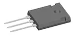


 工商网监
湘ICP备2023018690号
工商网监
湘ICP备2023018690号
