物料型号:DSA30I150PA
器件简介:
- 该器件是IXYS公司生产的第二代肖特基二极管,具有高性能、低损耗和软恢复特性。
- 它是一个单二极管,具有非常低的正向电压降(Vf)、极低的开关损耗、低Irm值、改进的热行为、高可靠性的电路操作以及降低的电压峰值,从而减少了保护电路的需求。
- 它还具有低噪声开关特性。
引脚分配:
- 背面为阴极。
参数特性:
- 最大非重复反向阻断电压(VRSM):150V
- 最大重复反向阻断电压(VRRM):150V
- 反向电流(I):在150V下,最小值为450A;在125°C时,最小值为5mA
- 正向电压降(VF):在30A时,典型值为0.8V;在60A时,典型值为0.93V
- 平均正向电流(IFAV):在150°C时,典型值为30A
- 阈值电压(VFo):用于功率损耗计算,典型值为0.55V
- 斜率电阻(Ro max):最大值为2.8mΩ
- 热阻(RthJc):从结到外壳的热阻,典型值为0.85K/W
- 热阻(RthCH):从外壳到散热器的热阻,典型值为0.5K/W
- 总功耗(Ptot):在25°C时,典型值为175W
- 最大正向浪涌电流:在10ms(50Hz)正弦波条件下,典型值为390A
- 结电容(C):在12V和1MHz时,典型值为289pF
功能详解:
- 该二极管适用于开关模式电源(SMPS)中的整流器和低压转换器中的自由轮二极管。
应用信息:
- 适用于开关模式电源(SMPS)的整流器和低压转换器中的自由轮二极管。
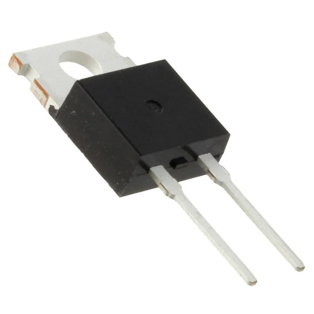
封装信息:
- 封装类型:TO-220
- 符合工业标准外形
- 符合RoHS指令
- 环氧树脂符合UL 94V-0标准
免责声明:
- 提供的信息被认为是准确和可靠的,但用户应独立评估并测试每个选定产品的适用性。Littelfuse产品不适用于所有应用。有关完整的免责声明通知,请访问www.littelfuse.com/disclaimer-electronics。
数据来源:
- 根据IEC 60747和半导体标准,除非另有说明。


 工商网监
湘ICP备2023018690号
工商网监
湘ICP备2023018690号
