Advance Technical Information
High Voltage,
High Frequency,
BiMOSFETTM Monolithic
Bipolar MOS Transistor
IXBF15N300C
VCES = 3000V
IC110 = 15A
VCE(sat) 6.0V
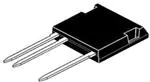
(Electrically Isolated Tab)
ISOPLUS i4-PakTM
Symbol
Test Conditions
Maximum Ratings
VCES
TJ
= 25°C to 150°C
3000
V
VCGR
TJ
= 25°C to 150°C, RGE = 1M
3000
V
VGES
Continuous
± 20
V
VGEM
Transient
± 30
V
1
5
IC25
TC = 25°C
37
A
IC110
TC = 110°C
15
A
ICM
TC = 25°C, 1ms
300
A
SSOA
(RBSOA)
VGE = 15V, TVJ = 125°C, RG = 10
Clamped Inductive Load
ICM = 120
VCES 1500
A
V
TSC
(SCSOA)
VGE = 15V, TJ = 125°C,
RG = 52, VCE = 1500V, Non-Repetitive
10
μs
PC
TC
300
W
-55 ... +150
°C
TJM
150
°C
Tstg
-55 ... +150
°C
300
260
°C
°C
20..120 / 4.5..27
N/lb.
4000
V~
5
g
= 25°C
TJ
TL
TSOLD
Maximum Lead Temperature for Soldering
Plastic Body for 10s
FC
Mounting Force
VISOL
50/60Hz, 5 Seconds
Weight
Symbol Test Conditions
(TJ = 25°C Unless Otherwise Specified)
IC
= 250μA, VGE = 0V
3000
VGE(th)
IC
= 250μA, VCE = VGE
3.0
ICES
VCE = VCES, VGE = 0V
IGES
VCE = 0V, VGE = ± 20V
VCE(sat)
IC
V
Note 2, TJ = 125°C
= 15A, VGE = 15V, Note 1
4.7
TJ = 125°C
© 2013 IXYS CORPORATION, All Rights Reserved
5.0
1 = Gate
2 = Emitter
Isolated Tab
5 = Collector
Features
Silicon Chip on Direct-Copper Bond
(DCB) Substrate
Isolated Mounting Surface
4000V~ Electrical Isolation
High Blocking Voltage
High Frequency Operation
Advantages
Low Gate Drive Requirement
High Power Density
Applications
Characteristic Values
Min.
Typ.
Max.
BVCES
2
5.0
V
25
5
μA
mA
±200
nA
6.0
V
Switch-Mode and Resonant-Mode
Power Supplies
V
DS100536(04/13)
�IXBF15N300C
Symbol Test Conditions
(TJ = 25°C Unless Otherwise Specified)
Characteristic Values
Min.
Typ.
Max.
gfs
18
IC = 15A, VCE = 10V, Note 1
Cies
Coes
Cres
VCE = 25V, VGE = 0V, f = 1MHz
Qg(on)
Qge
Qgc
IC = 15A, VGE = 15V, VCE = 1000V
td(on)
tri
Eon
td(off)
tfi
Eoff
td(on)
tri
Eon
td(off)
tfi
Eoff
Inductive load, TJ = 25°C
IC = 15A, VGE = 15V
VCE = 1500V, RG = 10
Note 3
Inductive load, TJ = 125°C
IC = 15A, VGE = 15V
VCE = 1500V, RG = 10
Note 3
RthJC
RthCS
ISOPLUS i4-PakTM (HV) Outline
30
S
6230
260
93
pF
pF
pF
267
33
99
nC
nC
nC
40
23
9.15
455
90
1.40
ns
ns
mJ
ns
ns
mJ
38
20
9.15
515
150
2.75
ns
ns
mJ
ns
ns
mJ
0.15
0.42 °C/W
°C/W
Pin 1 = Gate
Pin2 = Emitter
Pin 3 = Collector
Tab 4 = Isolated
Reverse Diode
Symbol Test Conditions
(TJ = 25°C Unless Otherwise Specified)
Characteristic Values
Min.
Typ.
Max
VF
IF = 15A, VGE = 0V, Note 1
trr
IF = 15A, VGE = 0V, -diF/dt = 100A/μs
IRM
QRM
Notes:
5.0
VR = 100V, VGE = 0V
V
706
ns
26
A
9.2
μC
1. Pulse test, t 300μs, duty cycle, d 2%.
2. Device must be heatsunk for high-temperature leakage current
measurements to avoid thermal runaway.
3. Switching times & energy losses may increase for higher VCE(clamp), TJ or RG.
ADVANCE TECHNICAL INFORMATION
The product presented herein is under development. The Technical Specifications offered are derived
from a subjective evaluation of the design, based upon prior knowledge and experience, and constitute a
"considered reflection" of the anticipated result. IXYS reserves the right to change limits, test
conditions, and dimensions without notice.
IXYS Reserves the Right to Change Limits, Test Conditions and Dimensions.
IXYS MOSFETs and IGBTs are covered
4,835,592
by one or more of the following U.S. patents: 4,860,072
4,881,106
4,931,844
5,017,508
5,034,796
5,049,961
5,063,307
5,187,117
5,237,481
5,381,025
5,486,715
6,162,665
6,259,123 B1
6,306,728 B1
6,404,065 B1
6,534,343
6,583,505
6,683,344
6,727,585
7,005,734 B2
6,710,405 B2 6,759,692
7,063,975 B2
6,710,463
6,771,478 B2 7,071,537
7,157,338B2
�IXBF15N300C
Fig. 2. Extended Output Characteristics @ T J = 25ºC
Fig. 1. Output Characteristics @ T J = 25ºC
30
220
VGE = 15V
9V
25
200
7V
VGE = 15V
13V
180
9V
160
15
IC - Amperes
IC - Amperes
20
6V
10
140
120
100
80
7V
60
40
5
6V
20
5V
0
0
0
1
2
3
4
5
6
7
0
5
10
20
25
Fig. 4. Dependence of VCE(sat) on
Junction Temperature
Fig. 3. Output Characteristics @ T J = 125ºC
30
1.5
VGE = 15V
9V
7V
25
15
VCE - Volts
VCE - Volts
VGE = 15V
1.4
I
C
= 30A
IC - Amperes
20
VCE(sat) - Normalized
1.3
6V
15
10
1.2
I
1.1
1.0
0.9
0.8
5
5V
= 15A
C
I
C
= 7.5A
0.7
0
0.6
0
1
2
3
4
5
6
7
8
-50
-25
VCE - Volts
0
25
50
75
100
125
150
TJ - Degrees Centigrade
Fig. 5. Collector-to-Emitter Voltage
vs. Gate-to-Emitter Voltage
Fig. 6. Input Admittance
50
10
45
TJ = 25ºC
9
40
35
IC - Amperes
VCE - Volts
8
7
I
6
5
C
= 30A
30
25
TJ = 125ºC
25ºC
- 40ºC
20
15
15A
10
4
5
7.5A
0
3
5
6
7
8
9
10
11
12
VGE - Volts
© 2013 IXYS CORPORATION, All Rights Reserved
13
14
15
4.0
4.5
5.0
5.5
VGE - Volts
6.0
6.5
7.0
�IXBF15N300C
Fig. 7. Transconductance
Fig. 8. Gate Charge
70
16
TJ = - 40ºC
60
25ºC
VGE - Volts
g f s - Siemens
50
40
125ºC
30
14
VCE = 1000V
12
I G = 10mA
I C = 15A
10
8
6
20
4
10
2
0
0
10
20
30
40
0
50
0
40
80
120
IC - Amperes
160
200
280
Fig. 10. Capacitance
Fig. 9. Forward Voltage Drop of Intrinsic Diode
10,000
50
TJ = 25ºC
J
Cies
----Capacitance - PicoFarads
125ºC
40
IF - Amperes
240
QG - NanoCoulombs
30
20
VGE = 0V
10
1,000
Coes
100
Cres
VGE = 15V
f = 1 MHz
0
0
1
2
3
4
5
6
7
8
10
9
0
5
10
15
20
25
30
35
40
VCE - Volts
VF - Volts
Fig. 12. Maximum Transient Thermal Impedance
Fig. 11. Reverse-Bias Safe Operating Area
1
140
120
Z(th)JC - ºC / W
IC - Amperes
100
80
60
0.1
0.01
40
TJ = 125ºC
20
0
300
RG = 10Ω
dv / dt < 10V / ns
600
900
1200
1500
1800
2100
2400
2700
3000
VCE - Volts
IXYS Reserves the Right to Change Limits, Test Conditions and Dimensions.
0.001
0.00001
0.0001
0.001
0.01
0.1
Pulse Width - Seconds
1
10
100
�IXBF15N300C
Fig. 13. Forward-Bias Safe Operating Area @ TC = 25ºC
Fig. 14. Forward-Bias Safe Operating Area @ TC = 75ºC
1000
1000
VCE(sat) Limit
VCE(sat) Limit
100
100
IC - Amperes
IC - Amperes
25µs
10
100µs
1ms
1
25µs
10
100µs
1ms
1
10ms
TJ = 150ºC
0.1
TC = 25ºC
TC = 75ºC
Single Pulse
100ms
DC
Single Pulse
10ms
TJ = 150ºC
0.1
0.01
DC
1
10
100
1,000
10,000
1
10
100
VCE - Volts
8
---
5
25
4
16
3
Eoff - MilliJoules
20
= 30A
3
2
10
TJ = 25ºC
12
I
2
C
1
= 15A
4
10
15
20
25
5
8
1
30
35
40
45
0
50
0
14
16
18
20
RG - Ohms
6
Eon -
Eoff
24
26
28
30
Fig. 18. Inductive Turn-off Switching Times vs.
Gate Resistance
2000
190
28
5
22
IC - Amperes
Fig. 17. Inductive Switching Energy Loss vs.
Junction Temperature
tf i
--24
RG = 10Ω , VGE = 15V
180
2
I
C
C
= 30A
16
12
= 15A
1
8
1400
t f i - Nanoseconds
I
3
1600
VCE = 1500V
1200
170
I
160
C
= 15A
I
C
1000
= 30A
800
600
400
150
200
0
25
35
45
55
65
75
85
95
105
TJ - Degrees Centigrade
© 2013 IXYS CORPORATION, All Rights Reserved
115
4
125
140
0
10
15
20
25
30
RG - Ohms
35
40
45
50
t d(off) - Nanoseconds
20
Eon - MilliJoules
4
1800
t d(off) - - - -
TJ = 125ºC, VGE = 15V
VCE = 1500V
Eoff - MilliJoules
15
TJ = 125ºC
Eon - MilliJoules
C
Eon - MilliJoules
I
20
VCE = 1500V
24
5
---
TJ = 125ºC , VGE = 15V
4
VCE = 1500V
Eon -
Eoff
28
TJ = 125ºC , VGE = 15V
6
Eoff - MilliJoules
Eon -
10,000
Fig. 16. Inductive Switching Energy Loss vs.
Collector Current
32
Eoff
1,000
VCE - Volts
Fig. 15. Inductive Switching Energy Loss vs.
Gate Resistance
7
100ms
0.01
�IXBF15N300C
Fig. 19. Inductive Turn-off Switching Times vs.
Collector Current
Fig. 20. Inductive Turn-off Switching Times vs.
Junction Temperature
240
t d(off) - - - -
RG = 10Ω , VGE = 15V
200
540
200
160
480
TJ = 125ºC
140
460
120
440
100
TJ = 25ºC
80
60
14
16
18
20
22
24
26
28
tfi
t d(off) - - - -
VCE = 1500V
180
480
140
460
I C = 15A
120
440
I C = 30A
420
100
420
400
80
400
380
60
30
25
35
45
55
80
I
C
= 15A
20
40
0
25
30
380
125
35
40
45
t d(on) - - - 46
RG = 10Ω , VGE = 15V
35
44
TJ = 25ºC
30
42
25
40
TJ = 125ºC
20
0
20
115
VCE = 1500V
t r i - Nanoseconds
= 30A
40
15
105
38
15
50
36
14
RG - Ohms
t d(on) - Nanoseconds
120
t d(on) - Nanoseconds
t r i - Nanoseconds
40
160
VCE = 1500V
10
95
48
tr i
t d(on) - - - -
TJ = 125ºC, VGE = 15V
C
85
45
200
I
75
Fig. 22. Inductive Turn-on Switching Times vs.
Collector Current
100
60
65
TJ - Degrees Centigrade
Fig. 21. Inductive Turn-on Switching Times vs.
Gate Resistance
80
500
160
IC - Amperes
tr i
520
t d(off) - Nanoseconds
500
t d(off) - Nanoseconds
180
540
RG = 10Ω , VGE = 15V
520
VCE = 1500V
t f i - Nanoseconds
220
t f i - Nanoseconds
tfi
220
560
16
18
20
22
24
26
28
30
IC - Amperes
Fig. 23. Inductive Turn-on Switching Times vs.
Junction Temperature
45
48
tr i
40
t d(on) - - - 46
RG = 10Ω , VGE = 15V
35
44
IC = 30A
30
25
42
40
20
t d(on) - Nanoseconds
t r i - Nanoseconds
VCE = 1500V
38
IC = 15A
15
25
35
45
55
65
75
85
95
105
115
36
125
TJ - Degrees Centigrade
IXYS Reserves the Right to Change Limits, Test Conditions and Dimensions.
IXYS REF: B_15N300C(9T)04-26-13
�