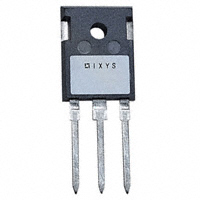
IXBH 40N160
High Voltage BIMOSFETTM
Monolithic Bipolar
MOS Transistor
IC25
= 33 A
VCES = 1600 V
VCE(sat) = 6.2 V typ.
tfi
= 40 ns
N-Channel, Enhancement Mode
C
TO-247 AD
G
C
E
G
C (TAB)
E
G = Gate,
E = Emitter,
Conditions
Maximum Ratings
VCES
VCGR
TJ = 25°C to 150°C
TJ = 25°C to 150°C; RGE = 1 MΩ
VGES
VGEM
Continuous
Transient
IC25
IC90
ICM
TC = 25°C
TC = 90°C
TC = 25°C, 1 ms
SSOA
(RBSOA)
VGE = 15 V, TVJ = 125°C, RG = 22 Ω VCE = 0.8·VCES
Clamped inductive load, L = 100 µH
PC
TC = 25°C
TJ
TJM
Tstg
TL
1.6 mm (0.063 in) from case for 10 s
Md
Mounting torque
1600
1600
V
V
±20
±30
V
V
33
20
40
A
A
A
ICM = 40
A
350
W
-55 ... +150
150
-55 ... +150
300
°C
°C
°C
°C
1.15/10Nm/lb.in.
Weight
Symbol
6
Conditions
Characteristic Values
(TJ = 25°C, unless otherwise specified)
min. typ. max.
BVCES
IC
= 1 mA, VGE = 0 V
1600
VGE(th)
IC
= 2 mA, VCE = VGE
4
ICES
VCE = 0.8·VCES
VGE = 0 V
IGES
VCE = 0 V, VGE = ±20 V
VCE(sat)
IC
V
8
TJ = 25°C
TJ = 125°C
= IC90, VGE = 15 V
6.2
TJ = 125°C
IXYS reserves the right to change limits, test conditions and dimensions.
© 2006 IXYS All rights reserved
g
V
400
3
µA
mA
± 500
nA
7.1
7.8
V
V
Features
• International standard package
JEDEC TO-247 AD
• High Voltage BIMOSFETTM
- replaces high voltage Darlingtons
and series connected MOSFETs
- lower effective RDS(on)
• Monolithic construction
- high blocking voltage capability
- very fast turn-off characteristics
• MOS Gate turn-on
- drive simplicity
• Intrinsic diode
Applications
•
•
•
•
•
AC motor speed control
DC servo and robot drives
DC choppers
Uninterruptible power supplies (UPS)
Switched-mode and resonant-mode
power supplies
• CRT deflection
• Lamp ballasts
Advantages
• Easy to mount with 1 screw
(isolated mounting screw hole)
• Space savings
• High power density
0648
Symbol
C = Collector,
TAB = Collector
1-4
�IXBH 40N160
Symbol
Conditions
Cies
Coes
Cres
VCE = 25 V, VGE = 0 V, f = 1 MHz
Qg
td(on)
tri
td(off)
tfi
Characteristic Values
(TJ = 25°C, unless otherwise specified)
min. typ. max.
3300
220
30
pF
pF
pF
130
nC
200
60
270
ns
ns
ns
40
ns
0.25
0.35 K/W
K/W
IC = 20 A, VCE = 600 V, VGE = 15 V
Inductive load, TJ = 125°C
IC = IC90, VGE = 15 V, L = 100 µH,
VCE = 960 V, RG = 22 Ω
RthJC
RthCK
Reverse Conduction
Symbol
VF
Characteristic Values
(TJ = 25°C, unless otherwise specified)
Conditions
min.
IF = IC90, VGE = 0 V, Pulse test
t < 300 µs, duty cycle d < 2%
typ.
max.
2.5
5
V
TO-247 AD Outline
© 2006 IXYS All rights reserved
Millimeter
Min.
Max.
Inches
Min.
Max.
A
B
19.81
20.80
20.32
21.46
0.780
0.819
0.800
0.845
C
D
15.75
3.55
16.26
3.65
0.610
0.140
0.640
0.144
E
F
4.32
5.4
5.49
6.2
0.170
0.212
0.216
0.244
G
H
1.65
-
2.13
4.5
0.065
-
0.084
0.177
J
K
1.0
10.8
1.4
11.0
0.040
0.426
0.055
0.433
L
M
4.7
0.4
5.3
0.8
0.185
0.016
0.209
0.031
N
1.5
2.49
0.087
0.102
0648
IXYS reserves the right to change limits, test conditions and dimensions.
Dim.
2-4
�IXBH 40N160
70
70
VGE = 17V
TJ = 25°C
VGE = 17V
TJ = 125°C
60
60
15V
50
13V
IC - Amperes
IC - Amperes
15V
40
30
20
50
13V
40
30
20
10
10
0
0
0
2
4
6
8
10
12
14
16
0
18
2
4
8
10
12
14
16
18
VCE - Volts
VCE - Volts
Fig. 1 Typ. Output Characteristics
Fig. 2 Typ. Output Characteristics
70
70
VCE = 20V
60
60
50
50
IF - Amperes
IC - Amperes
6
40
TJ = 25°C
TJ = 125°C
30
40
30
TJ = 25°C
20
20
10
10
0
0.0
0
5
6
7
8
9
10
11
12
13
0.5
1.0
VGE - Volts
2.5
3.0
3.5
4.0
Fig. 4 Typ. Characteristics of Reverse
Conduction
100
VCE = 600V
IC = 20A
14
2.0
VF - Volts
Fig. 3 Typ. Transfer Characteristics
16
1.5
TJ = 125°C
ICM - Amperes
VGE - Volts
12
10
8
6
10
TJ = 125°C
VCEK < VCES
IXBH 40N140
IXBH 40N160
1
4
2
0
20
40
60
80
100
120
140
QG - nanocoulombs
Fig. 5 Typ. Gate Charge characteristics
IXYS reserves the right to change limits, test conditions and dimensions.
© 2006 IXYS All rights reserved
0.1
0
400
800
1200
1600
VCE - Volts
Fig. 6 Reverse Based Safe Operating Area
RBSOA
0648
0
3-4
�IXBH 40N160
400
VCE = 960V
VGE = 15V
IC = 20A
TJ = 125°C
VCE = 960V
VGE = 15V
40 RG = 22Ω
td(off) - nanoseconds
tfi - nanoseconds
50
TJ = 125°C
30
20
10
300
200
100
0
0
0
10
20
30
40
0
10
20
30
40
RG - Ohms
IC - Amperes
Fig. 7 Typ. Fall Time
Fig. 8 Typ. Turn Off Delay Time
1
ZthJC - K/W
0.1
0.01
Single Pulse
0.001
0.0001
0.00001
IXBH40
0.0001
0.001
0.01
0.1
1
Pulse Width - Seconds
IXYS reserves the right to change limits, test conditions and dimensions.
© 2006 IXYS All rights reserved
0648
Fig. 9 Typ. Transient Thermal Impedance
4-4
�Disclaimer Notice - Information furnished is believed to be accurate and reliable. However, users should independently
evaluate the suitability of and test each product selected for their own applications. Littelfuse products are not designed for,
and may not be used in, all applications.Read complete Disclaimer Notice at www.littelfuse.com/disclaimer-electronics.
�
很抱歉,暂时无法提供与“IXBH40N160”相匹配的价格&库存,您可以联系我们找货
免费人工找货