IXBK55N300
IXBX55N300
High Voltage, High Gain
BiMOSFETTM
VCES
IC110
= 3000V
= 55A
3.2V
VCE(sat)
Monolithic Bipolar
MOS Transistor
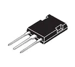
TO-264
(IXBK)
Symbol
Test Conditions
Maximum Ratings
VCES
TJ = 25°C to 150°C
3000
V
VCGR
TJ = 25°C to 150°C, RGE = 1M
3000
V
VGES
Continuous
±25
V
VGEM
Transient
±35
V
IC25
IC110
ICM
TC = 25°C (Chip Capability)
TC = 110°C
TC = 25°C, 1ms
130
55
600
A
A
A
SSOA
VGE = 15V, TVJ = 125°C, RG = 2
ICM = 110
A
(RBSOA)
Clamped Inductive Load
1500
V
TSC
(SCSOA)
VGE = 15V, TJ = 125°C,
RG = 10, VCE = 1250V, Non-Repetitive
10
µs
PC
TC = 25°C
625
W
-55 ... +150
°C
TJM
150
°C
Tstg
-55 ... +150
°C
TJ
TL
Maximum Lead Temperature for Soldering
1.6 mm (0.062 in.) from Case for 10
Md
FC
Mounting Torque (TO-264)
Mounting Force (PLUS247)
Weight
TO-264
PLUS247
300
°C
1.13/10
20..120/4.5..27
Nm/lb.in
N/lb
10
6
g
g
G
C
E
PLUS247
(IXBX)
G
IC
= 1mA, VGE = 0V
3000
VGE(th)
IC
= 4mA, VCE = VGE
3.0
ICES
VCE = VCES, VGE = 0V
5.0
VCE = 0V, VGE = ± 25V
VCE(sat)
IC
= 55A, VGE = 15V, Note 1
TJ = 125C
© 2021 Littelfuse, Inc.
V
50 µA
TJ = 125C
IGES
V
3 mA
±200 nA
3.2
V
V
E
= Emitter
Tab = Collector
High Blocking Voltage
International Standard Packages
Low Conduction Losses
High Current Handling Capability
MOS Gate Turn-On
- Drive Simplicity
Easy to Mount
Space Savings
High Power Density
Applications
2.7
3.3
Tab
E
Advantages
BVCES
C
Features
Characteristic Values
Min.
Typ.
Max.
G
G = Gate
C = Collector
Symbol
Test Conditions
(TJ = 25C, Unless Otherwise Specified)
Tab
Uninterruptible Power Supplies (UPS)
Switch-Mode and Resonant-Mode
Power Supplies
Capacitor Discharge Circuits
Laser Generators
DS100158B(7/21)
�IXBK55N300
IXBX55N300
Symbol Test Conditions
(TJ = 25°C Unless Otherwise Specified)
gfS
Characteristic Values
Min.
Typ.
Max.
IC = 55A, VCE = 10V, Note 1
32
Cies
Coes
VCE = 25V, VGE = 0V, f = 1MHz
Cres
Qg
Qge
IC = 55A, VGE = 15V, VCE = 1000V
Qgc
td(on)
tr
td(off)
tf
td(on)
tr
td(off)
tf
Resistive Switching Times, TJ = 25°C
IC = 110A, VGE = 15V
VCE = 1250V, RG = 2
Resistive Switching Times, TJ = 125°C
IC = 110A, VGE = 15V
VCE = 1250V, RG = 2
50
S
7300
pF
275
pF
83
pF
335
nC
47
nC
130
nC
54
ns
307
ns
230
ns
268
ns
52
ns
585
ns
215
ns
260
ns
RthJC
0.20 °C/W
RthCS
0.15
°C/W
Reverse Diode
Symbol Test Conditions
(TJ = 25°C Unless Otherwise Specified)
Characteristic Values
Min.
Typ.
Max
VF
IF = 55A, VGE = 0V, Note 1
trr
IF = 28A, VGE = 0V, -diF/dt = 100A/µs
1.9
µs
IRM
VR = 100V, VGE = 0V
54
A
Note
2.5
V
1: Pulse Test, t 300µs, Duty Cycle, d 2%.
Additional provisions for lead-to-lead isolation are required at V CE > 1250V.
Littelfuse reserves the right to change limits, test conditions, and dimensions.
IXYS MOSFETs and IGBTs are covered
by one or moreof the following U.S. patents:
4,835,592
4,860,072
4,881,106
4,931,844
5,017,508
5,034,796
5,049,961
5,063,307
5,187,117
5,237,481
5,381,025
5,486,715
6,162,665
6,259,123 B1
6,306,728 B1
6,404,065 B1
6,534,343
6,583,505
6,683,344
6,710,405 B2
6,710,463
6,727,585
7,005,734 B2
6,759,692
7,063,975 B2
6,771,478 B2 7,071,537
7,157,338B2
�IXBK55N300
IXBX55N300
Fig. 2. Extended Output Characteristics @ TJ = 25ºC
Fig. 1. Output Characteristics @ TJ = 25ºC
120
300
VGE = 25V
20V
15V
100
V GE = 25V
20V
15V
80
I C - Amperes
I C - Amperes
250
10V
60
40
200
10V
150
100
20
50
5V
5V
0
0
0.5
1
1.5
2
2.5
3
3.5
0
4
0
2
3
4
5
6
VCE - Volts
Fig. 3. Output Characteristics @ TJ = 125ºC
Fig. 4. Dependence of VCE(sat) on
Junction Temperature
120
7
8
125
150
1.8
V GE = 25V
20V
15V
VGE = 15V
1.6
VCE(sat) - Normalized
100
80
I C - Amperes
1
VCE - Volts
10V
60
40
I C = 110A
1.4
1.2
I C = 55A
1.0
I C = 27.5A
20
0.8
5V
0
0
0.5
1
1.5
2
2.5
3
3.5
4
4.5
0.6
5
-50
-25
0
VCE - Volts
25
50
75
100
TJ - Degrees Centigrade
Fig. 5. Collector-to-Emitter Voltage
vs. Gate-to-Emitter Voltage
Fig. 6. Input Admittance
180
5.5
TJ = 25ºC
5.0
160
140
120
4.0
I C - Amperes
VCE - Volts
4.5
I C = 110A
3.5
100
80
TJ = 125ºC
25ºC
- 40ºC
60
55A
3.0
40
2.5
20
27.5A
0
2.0
5
6
7
8
9
10
VGE - Volts
© 2021 Littelfuse, Inc.
11
12
13
14
15
3.0
3.5
4.0
4.5
5.0
5.5
6.0
6.5
VGE - Volts
7.0
7.5
8.0
8.5
9.0
�IXBK55N300
IXBX55N300
Fig. 8. Forward Voltage Drop of Intrinsic Diode
Fig. 7. Transconductance
180
100
TJ = - 40ºC
90
160
80
140
25ºC
60
120
I F - Amperes
g f s - Siemens
70
125ºC
50
40
TJ = 25ºC
100
TJ = 125ºC
80
60
30
40
20
20
10
0
0
0
20
40
60
80
100
120
140
160
180
0.4
200
0.6
0.8
1.0
1.2
1.4
1.6
I C - Amperes
2.4
2.6
2.8
3.0
f = 1 MHz
VCE = 1000V
I C = 55A
I G = 10mA
Capacitance - PicoFarads
VGE - Volts
2.2
100,000
16
12
2.0
Fig. 10. Capacitance
Fig. 9. Gate Charge
14
1.8
VF - Volts
10
8
6
4
10,000
Cies
1,000
C oes
100
Cres
2
10
0
0
50
100
150
200
250
300
0
350
5
10
15
20
25
30
35
40
VCE - Volts
QG - NanoCoulombs
Fig. 12. Maximum Transient Thermal Impedance
Fig. 11. Reverse-Bias Safe Operating Area
1
120
100
0.1
Z(th)JC - K / W
I C - Amperes
80
60
40
0.01
TJ = 125ºC
RG = 2Ω
dv / dt < 10V / ns
20
0
250
750
1250
1750
2250
2750
VCE - Volts
Littelfuse reserves the right to change limits, test conditions, and dimensions.
0.001
0.0001
0.001
0.01
0.1
Pulse Width - Seconds
1
10
�IXBK55N300
IXBX55N300
Fig. 14. Resistive Turn-on Rise Time vs.
Collector Current
Fig. 13. Resistive Turn-on Rise Time vs.
Junction Temperature
700
700
RG = 2Ω , VGE = 15V
VCE = 1250V
600
600
500
t r - Nanoseconds
t r - Nanoseconds
TJ = 125ºC
I C = 220A
400
I C = 110A
300
500
RG = 2Ω , VGE = 15V
VCE = 1250V
400
TJ = 25ºC
300
200
200
25
35
45
55
65
75
85
95
105
115
125
40
60
80
100
120
720
80
620
70
I C = 110A
60
580
560
3
4
5
6
7
8
9
10
11
12
13
14
280
260
240
280
220
I C = 110A
270
200
260
180
I C = 220A
250
160
50
240
140
40
230
120
25
35
45
55
65
75
85
95
105
115
RG - Ohms
TJ - Degrees Centigrade
Fig. 17. Resistive Turn-off Switching Times vs.
Collector Current
Fig. 18. Resistive Turn-off Switching Times vs.
Gate Resistance
360
320
tf
340
RG = 2Ω, VGE = 15V
VCE = 1250V
td(off)
300
240
280
220
260
200
240
180
160
TJ = 125ºC, 25ºC
200
140
60
80
100
120
140
I C - Amperes
© 2021 Littelfuse, Inc.
160
180
200
220
680
td(off)
600
320
520
I C = 110A
300
440
280
360
I C = 220A
260
280
240
200
220
120
2
3
4
5
6
7
8
9
RG - Ohms
10
11
12
13
14
15
t d(off) - Nanoseconds
300
t d(off) - Nanoseconds
260
125
TJ = 125ºC, VGE = 15V
VCE = 1250V
280
320
220
tf
340
t f - Nanoseconds
360
40
td(off)
290
15
380
t f - Nanoseconds
t f - Nanoseconds
I C = 220A
2
tf
t d(off) - Nanoseconds
90
600
220
RG = 2Ω, VGE = 15V
VCE = 1250V
300
100
660
640
200
300
310
110
t d(on) - Nanoseconds
t r - Nanoseconds
td(on)
TJ = 125ºC, VGE = 15V
VCE = 1250V
680
180
320
120
tr
160
Fig. 16. Resistive Turn-off Switching Times vs.
Junction Temperature
Fig. 15. Resistive Turn-on Switching Times vs.
Gate Resistance
700
140
I C - Amperes
TJ - Degrees Centigrade
�IXBK55N300
IXBX55N300
Fig. 19. Forward-Bias Safe Operating Area
@ TC = 25ºC
Fig. 20. Forward-Bias Safe Operating Area
@ TC = 75ºC
1000
1000
VCE(sat) Limit
VCE(sat) Limit
100
100
25µs
25µs
10
I D - Amperes
I D - Amperes
100µs
1ms
1
100µs
10
1ms
1
10ms
TJ = 150ºC
TC = 25ºC
Single Pulse
0.1
100ms
DC
0.01
10ms
TJ = 150ºC
TC = 75ºC
Single Pulse
0.1
100ms
DC
0.01
1
10
100
1,000
10,000
VDS - Volts
1
10
100
1,000
10,000
VDS - Volts
Littelfuse reserves the right to change limits, test conditions, and dimensions.
IXYS REF: B_55N300 (8T) 6-23-21
�IXBK55N300
IXBX55N300
TO-264 Outline
D
B
E
A
Q S
0R
Q1
D
0R1
1
2
L1
3
C
L
A1
b1
J M C AM
b
b2
c
e
= Gate
2,4 = Collector
3 = Emitter
1
0P1
BACK SIDE
A
K M D BM
0P
4
PLUS247TM Outline
A
E
A2
E1
Q
D2
R
D
1
2
4
3
L1
L
A1
b
e
b2
3 PLCS
C
b4
1 = Gate
2,4 = Collector
3 = Emitter
© 2021 Littelfuse, Inc.
2 PLCS
2 PLCS
�IXBK55N300
IXBX55N300
Disclaimer Notice - Information furnished is believed to be accurate and reliable. However, users should independently
evaluate the suitability of and test each product selected for their own applications. Littelfuse products are not designed for,
and may not be used in, all applications. Read complete Disclaimer Notice at www.littelfuse.com/disclaimer-electronics.
Littelfuse reserves the right to change limits, test conditions, and dimensions.
�


 工商网监
湘ICP备2023018690号
工商网监
湘ICP备2023018690号
