IXFA230N075T2
IXFP230N075T2
TrenchT2TM HiperFETTM
Power MOSFET
VDSS
ID25
RDS(on)
N-Channel Enhancement Mode
Avalanche Rated
Fast Intrinsic Rectifier
= 75V
= 230A
Ω
≤ 4.2mΩ
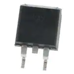
TO-263 AA (IXFA)
G
S
D (Tab)
Symbol
Test Conditions
Maximum Ratings
VDSS
TJ = 25°C to 175°C
75
V
VDGR
TJ = 25°C to 175°C, RGS = 1MΩ
75
V
VGSM
Transient
± 20
V
ID25
TC = 25°C (Chip Capability)
230
A
ILRMS
Lead Current Limit, RMS
120
A
IDM
TC = 25°C, Pulse Width Limited by TJM
700
A
IA
TC = 25°C
115
A
EAS
TC = 25°C
850
mJ
PD
TC = 25°C
480
W
-55 ... +175
°C
TJM
175
°C
Tstg
-55 ... +175
°C
300
260
°C
°C
1.13 / 10
Nm/lb.in.
2.5
3.0
g
g
TJ
TL
Tsold
1.6mm (0.062in.) from Case for 10s
Plastic Body for 10 seconds
Md
Mounting Torque (TO-220)
Weight
TO-263
TO-220
TO-220AB (IXFP)
G
DS
G = Gate
S = Source
D (Tab)
D
= Drain
Tab = Drain
Features
z
International Standard Packages
175°C Operating Temperature
z
High Current Handling Capability
z
Avalanche Rated
z
Fast Intrinsic Rectifier
z
Low RDS(on)
z
Advantages
z
z
Symbol
Test Conditions
(TJ = 25°C Unless Otherwise Specified)
z
Characteristic Values
Min.
Typ.
Max.
BVDSS
VGS = 0V, ID = 250μA
75
VGS(th)
VDS = VGS, ID = 1mA
2.0
IGSS
VGS = ± 20V, VDS = 0V
±200 nA
IDSS
VDS = VDSS, VGS = 0V
25 μA
TJ = 150°C
RDS(on)
VGS = 10V, ID = 50A, Note 1
© 2010 IXYS CORPORATION, All Rights Reserved
4.0
Easy to Mount
Space Savings
High Power Density
V
Applications
V
z
250 μA
4.2 mΩ
z
z
z
Automotive
- Motor Drives
- 12V Power Bus
- ABS Systems
DC/DC Converters and Off-Line UPS
Primary- Side Switch
High Current Switching Applications
DS100074A(03/10)
�IXFA230N075T2
IXFP230N075T2
Symbol
Test Conditions
(TJ = 25°C, Unless Otherwise Specified)
gfs
Characteristic Values
Min. Typ.
Max.
VDS = 10V, ID = 60A, Note 1
50
Ciss
Coss
VGS = 0V, VDS = 25V, f = 1MHz
85
S
10.5
nF
1165
pF
125
pF
23
ns
18
ns
33
ns
15
ns
178
nC
53
nC
41
nC
Crss
td(on)
tr
td(off)
Resistive Switching Times
VGS = 10V, VDS = 0.5 • VDSS, ID = 0.5 • ID25
RG = 2Ω (External)
tf
Qg(on)
Qgs
VGS = 10V, VDS = 0.5 • VDSS, ID = 0.5 • ID25
Qgd
0.31 °C/W
RthJC
RthCH
TO-263 (IXFA) Outline
TO-220
°C/W
0.50
Source-Drain Diode
Symbol
Test Conditions
(TJ = 25°C, Unless Otherwise Specified)
Characteristic Values
Min. Typ.
Max.
IS
VGS = 0V
230
A
ISM
Repetitive, Pulse Width Limited by TJM
900
A
VSD
IF = 100A, VGS = 0V, Note 1
1.3
V
trr
IF = 115A, VGS = 0V
IRM
QRM
Note
-di/dt = 100A/μs
VR = 37V
59
ns
3.6
A
106
nC
TO-220 (IXFP) Outline
1. Pulse test, t ≤ 300μs, duty cycle, d ≤ 2%.
Pins:
1 - Gate
3 - Source
2 - Drain
IXYS Reserves the Right to Change Limits, Test Conditions, and Dimensions.
IXYS MOSFETs and IGBTs are covered
4,835,592
by one or more of the following U.S. patents: 4,850,072
4,881,106
4,931,844
5,017,508
5,034,796
5,049,961
5,063,307
5,187,117
5,237,481
5,381,025
5,486,715
6,162,665
6,259,123 B1
6,306,728 B1
6,404,065 B1
6,534,343
6,583,505
6,683,344
6,727,585
7,005,734 B2
6,710,405 B2 6,759,692
7,063,975 B2
6,710,463
6,771,478 B2 7,071,537
7,157,338B2
�IXFA230N075T2
IXFP230N075T2
Fig. 1. Output Characteristics @ T J = 25ºC
Fig. 2. Extended Output Characteristics @ T J = 25ºC
240
320
VGS = 15V
10V
9V
200
280
ID - Amperes
7V
120
8V
240
8V
160
ID - Amperes
VGS = 15V
10V
9V
80
200
7V
160
120
6V
6V
80
40
40
5V
0
5V
0
0.0
0.1
0.2
0.3
0.4
0.5
0.6
0.7
0.8
0.9
0.0
1.0
0.5
1.0
1.5
2.5
3.0
3.5
4.0
4.5
Fig. 4. RDS(on) Normalized to ID = 115A Value vs.
Junction Temperature
Fig. 3. Output Characteristics @ T J = 150ºC
240
2.6
VGS = 15V
10V
9V
8V
2.4
VGS = 10V
2.2
R DS(on) - Normalized
200
160
ID - Amperes
2.0
VDS - Volts
VDS - Volts
7V
120
6V
80
2.0
1.8
I D = 230A
1.6
I D = 115A
1.4
1.2
1.0
0.8
40
5V
0.6
0
0.4
0.0
0.2
0.4
0.6
0.8
1.0
1.2
1.4
1.6
1.8
2.0
-50
-25
0
25
VDS - Volts
50
75
100
125
150
175
TJ - Degrees Centigrade
Fig. 5. RDS(on) Normalized to ID = 115A Value vs.
Drain Current
Fig. 6. Drain Current vs. Case Temperature
2.6
140
External Lead Current Limit
2.4
120
TJ = 175ºC
2.0
100
ID - Amperes
R DS(on) - Normalized
2.2
1.8
VGS = 10V
1.6
15V - - - -
1.4
1.2
80
60
40
1.0
20
TJ = 25ºC
0.8
0
0.6
0
50
100
150
200
ID - Amperes
© 2010 IXYS CORPORATION, All Rights Reserved
250
300
-50
-25
0
25
50
75
100
TC - Degrees Centigrade
125
150
175
200
�IXFA230N075T2
IXFP230N075T2
Fig. 8. Transconductance
Fig. 7. Input Admittance
160
140
140
120
TJ = - 40ºC
TJ = 150ºC
25ºC
- 40ºC
100
100
25ºC
80
150ºC
g f s - Siemens
ID - Amperes
120
80
60
60
40
40
20
20
0
0
3.5
4.0
4.5
5.0
5.5
6.0
0
6.5
20
40
60
VGS - Volts
270
9
240
8
210
7
180
6
VGS - Volts
IS - Amperes
10
150
120
TJ = 150ºC
120
140
160
VDS = 38V
I D = 115A
I G = 10mA
5
4
3
60
2
TJ = 25ºC
30
1
0
0
0.4
0.5
0.6
0.7
0.8
0.9
1.0
1.1
1.2
0
1.3
20
40
VSD - Volts
60
80
100
120
140
160
180
QG - NanoCoulombs
Fig. 11. Capacitance
Fig. 12. Forward-Bias Safe Operating Area
100,000
1000
RDS(on) Limit
f = 1 MHz
Ciss
25µs
10,000
100
ID - Amperes
Capacitance - PicoFarads
100
Fig. 10. Gate Charge
Fig. 9. Forward Voltage Drop of Intrinsic Diode
300
90
80
ID - Amperes
Coss
1,000
100µs
External Lead Current Limit
1ms
10
10ms
Crss
DC
100
1
0
5
10
15
20
25
30
35
40
VDS - Volts
IXYS Reserves the Right to Change Limits, Test Conditions, and Dimensions.
1
10
VDS - Volts
100ms
100
�IXFA230N075T2
IXFP230N075T2
Fig. 14. Resistive Turn-on Rise Time vs.
Drain Current
Fig. 13. Resistive Turn-on Rise Time vs.
Junction Temperature
22
26
RG = 2Ω , VGS = 10V
RG = 2Ω , VGS = 10V
24
VDS = 38V
20
VDS = 38V
20
I
t r - Nanoseconds
t r - Nanoseconds
22
= 230A
D
18
16
I
D
= 115A
18
TJ = 25ºC
16
14
14
TJ = 125ºC
12
12
10
110
10
25
35
45
55
65
75
85
95
105
115
125
120
130
140
150
TJ - Degrees Centigrade
50
28
tf
26
RG = 2Ω, VGS = 10V
40
25
30
20
25
15
20
10
15
12
10
10
5
6
8
10
12
14
45
20
40
18
35
16
30
20
25
35
45
55
RG = 2Ω, VGS = 10V
VDS = 38V
60
280
55
240
40
16
35
14
30
TJ = 25ºC
12
140
150
160
170
180
190
200
ID - Amperes
© 2010 IXYS CORPORATION, All Rights Reserved
210
220
25
20
230
t f - Nanoseconds
45
18
130
85
95
105
115
15
125
280
tf
td(off) - - - -
240
TJ = 125ºC, VGS = 10V
VDS = 38V
200
200
I D = 115A
160
160
120
120
80
80
40
I
D
40
= 230A
0
0
2
4
6
8
10
RG - Ohms
12
14
16
t d(off) - Nanoseconds
50
TJ = 125ºC
120
75
Fig. 18. Resistive Turn-off Switching Times vs.
Gate Resistance
t d(off) - Nanoseconds
t f - Nanoseconds
td(off) - - - -
20
10
110
65
TJ - Degrees Centigrade
26
22
25
I D = 230A
Fig. 17. Resistive Turn-off Switching Times vs.
Drain Current
24
50
I D = 115A
14
16
55
VDS = 38V
RG - Ohms
tf
230
60
td(off) - - - -
22
35
4
220
65
24
30
2
210
t d(off) - Nanoseconds
35
200
50
45
I D = 230A, 115A
VDS = 38V
190
30
t d(on) - Nanoseconds
t r - Nanoseconds
td(on) - - - -
TJ = 125ºC, VGS = 10V
40
180
55
t f - Nanoseconds
tr
170
Fig. 16. Resistive Turn-off Switching Times vs.
Junction Temperature
Fig. 15. Resistive Turn-on Switching Times vs.
Gate Resistance
45
160
ID - Amperes
�IXFA230N075T2
IXFP230N075T2
Fig. 19. Maximum Transient Thermal Impedance
Z (th )J C - ºC / W
1.000
0.100
0.010
0.001
0.00001
0.0001
0.001
0.01
0.1
1
10
Pulse Width - Seconds
IXYS Reserves the Right to Change Limits, Test Conditions, and Dimensions.
IXYS REF: T_230N075T2(V6)2-26-10-C
�Disclaimer Notice - Information furnished is believed to be accurate and reliable. However, users should independently
evaluate the suitability of and test each product selected for their own applications. Littelfuse products are not designed for,
and may not be used in, all applications. Read complete Disclaimer Notice at www.littelfuse.com/disclaimer-electronics.
�