PolarTM Power MOSFET
HiPerFETTM
IXFB40N110P
VDSS
ID25
RDS(on)
trr
N-Channel Enhancement Mode
Avalanche Rated
Fast Intrinsic Diode
=
=
≤
≤
1100V
40A
Ω
260mΩ
300ns
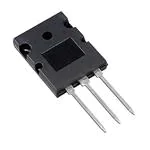
PLUS264TM (IXFB)
Symbol
Test Conditions
Maximum Ratings
VDSS
VDGR
TJ = 25°C to 150°C
TJ = 25°C to 150°C, RGS = 1MΩ
1100
1100
V
V
VGSS
Continuous
±30
V
VGSM
Transient
±40
V
ID25
TC = 25°C
40
A
IDM
TC = 25°C, pulse width limited by TJM
100
A
IAR
TC = 25°C
20
A
EAS
TC = 25°C
2
J
dV/dt
IS ≤ IDM, VDD ≤ VDSS, TJ ≤ 150°C
15
V/ns
PD
TC = 25°C
1250
W
-55 ... +150
150
-55 ... +150
°C
°C
°C
300
260
°C
°C
30..120/6.7..27
N/lb.
10
g
TJ
TJM
Tstg
TL
TSOLD
1.6mm (0.062 in.) from case for 10s
Plastic body for 10s
FC
Mounting force
Weight
G
D
(TAB)
S
G = Gate
S = Source
D = Drain
TAB = Drain
Features
z
z
z
Fast recovery diode
Unclamped Inductive Switching (UIS)
rated
Low package inductance
- easy to drive and to protect
Advantages
z
z
z
Plus 264TM package for clip or spring
mounting
Space savings
High power density
Applications:
z
Symbol
Test Conditions
(TJ = 25°C, unless otherwise specified)
Characteristic Values
Min.
Typ.
Max.
BVDSS
VGS = 0V, ID = 3mA
1100
VGS(th)
VDS = VGS, ID = 1mA
3.5
IGSS
VGS = ±30V, VDS = 0V
IDSS
VDS = VDSS
VGS = 0V
RDS(on)
VGS = 10V, ID = 0.5 • ID25, Note 1
z
z
V
6.5
V
±200
nA
50
3
μA
mA
260
mΩ
z
z
TJ = 125°C
© 2008 IXYS CORPORATION, All rights reserved
High Voltage Switched-mode and
resonant-mode power supplies
High Voltage Pulse Power Applications
High Voltage Discharge circuits in
Lasers Pulsers, Spark Igniters, RF
Generators
High Voltage DC-DC converters
High Voltage DC-AC inverters
DS99849B(03/08)
�IXFB40N110P
Symbol
Test Conditions
(TJ = 25°C, unless otherwise specified)
gfs
Characteristic Values
Min.
Typ.
Max.
VDS = 20V, ID = 0.5 • ID25, Note 1
20
Ciss
Coss
VGS = 0V, VDS = 25V, f = 1MHz
Crss
RGI
Gate Input Resistance
td(on)
Resistive Switching Times
tr
td(off)
tf
VGS = 10V, VDS = 0.5 • VDSS, ID =0.5 • ID25
RG = 1Ω (External)
Qg(on)
Qgs
VGS = 10V, VDS = 0.5 • VDSS, ID = 0.5 • ID25
Qgd
32
S
19
nF
1070
pF
46
pF
1.65
Ω
53
ns
55
ns
110
ns
54
ns
310
nC
95
nC
142
nC
RthJC
0.10
RthCS
Symbol
Test Conditions
IS
VGS = 0V
ISM
°C/W
°C/W
0.13
Source-Drain Diode
PLUS264TM (IXFB) Outline
Characteristic Values
(TJ = 25°C, unless otherwise specified)
Min.
Typ.
Max.
40
A
Repetitive, pulse width limited by TJM
160
A
VSD
IF = IS, VGS = 0V, Note 1
1.5
V
trr
QRM
IRM
300
IF = 20A, -di/dt = 100A/μs
VR = 100V, VGS = 0V
ns
μC
A
2.2
16
Note 1: Pulse test, t ≤ 300μs; duty cycle, d ≤ 2%.
IXYS reserves the right to change limits, test conditions, and dimensions.
IXYS MOSFETs and IGBTs are covered
4,835,592
by one or more of the following U.S. patents: 4,850,072
4,881,106
4,931,844
5,017,508
5,034,796
5,049,961
5,063,307
5,187,117
5,237,481
5,381,025
5,486,715
6,162,665
6,259,123 B1
6,306,728 B1
6,404,065 B1
6,534,343
6,583,505
6,683,344
6,727,585
7,005,734 B2
6,710,405 B2 6,759,692
7,063,975 B2
6,710,463
6,771,478 B2 7,071,537
7,157,338B2
�IXFB40N110P
Fig. 1. Output Characteristics
@ 25ºC
Fig. 2. Extended Output Characteristics
@ 25ºC
40
90
VGS = 10V
8V
35
70
ID - Amperes
30
ID - Amperes
VGS = 10V
8V
80
7V
25
20
15
60
50
7V
40
30
6V
10
5
20
6V
10
5V
5V
0
0
0
1
2
3
4
5
6
7
8
0
9
5
10
40
25
30
3.0
VGS = 10V
7V
35
2.8
VGS = 10V
2.6
2.4
RDS(on) - Normalized
30
ID - Amperes
20
Fig. 4. RDS(on) Normalized to ID = 20A Value
vs. Junction Temperature
Fig. 3. Output Characteristics
@ 125ºC
25
6V
20
15
10
2.2
2.0
I D = 40A
1.8
I D = 20A
1.6
1.4
1.2
1.0
0.8
5
5V
0.6
0
0.4
0
2
4
6
8
10
12
14
16
18
20
22
-50
-25
0
VDS - Volts
25
50
75
100
125
150
TJ - Degrees Centigrade
Fig. 5. RDS(on) Normalized to ID = 20A Value
vs. Drain Current
Fig. 6. Maximum Drain Current vs.
Case Temperature
45
2.8
VGS = 10V
2.6
40
TJ = 125ºC
2.4
35
2.2
ID - Amperes
RDS(on) - Normalized
15
VDS - Volts
VDS - Volts
2.0
1.8
1.6
30
25
20
15
1.4
10
1.2
TJ = 25ºC
5
1.0
0
0.8
0
10
20
30
40
50
ID - Amperes
© 2008 IXYS CORPORATION, All rights reserved
60
70
80
90
-50
-25
0
25
50
75
TC - Degrees Centigrade
100
125
150
�IXFB40N110P
Fig. 7. Input Admittance
50
45
45
40
40
g f s - Siemens
55
50
35
ID - Amperes
Fig. 8. Transconductance
55
TJ = 125ºC
25ºC
- 40ºC
30
25
20
TJ = - 40ºC
25ºC
35
30
125ºC
25
20
15
15
10
10
5
5
0
0
3.5
4.0
4.5
5.0
5.5
6.0
6.5
7.0
0
7.5
5
10
VGS - Volts
20
25
30
35
40
45
50
55
ID - Amperes
Fig. 9. Forward Voltage Drop of
Intrinsic Diode
Fig. 10. Gate Charge
16
120
110
VDS = 550V
14
I D = 20A
100
I G = 10mA
12
90
80
VGS - Volts
IS - Amperes
15
70
60
50
40
10
8
6
TJ = 125ºC
30
4
TJ = 25ºC
20
2
10
0
0
0.3
0.4
0.5
0.6
0.7
0.8
0.9
1.0
1.1
1.2
0
50
100
VSD - Volts
150
200
250
300
350
400
450
QG - NanoCoulombs
Fig. 12. Maximum Transient Thermal
Impedance
Fig. 11. Capacitance
100,000
1.000
10,000
Ciss
Z(th)JC - ºC / W
Capacitance - PicoFarads
f = 1 MHz
1,000
Coss
0.100
0.010
100
Crss
10
0
5
10
15
20
25
30
35
40
VDS - Volts
0.001
0.0001
0.001
0.01
0.1
1
10
Pulse Width - Seconds
IXYS reserves the right to change limits, test conditions, and dimensions.
IXYS REF: F_40N110P(97) 03-28-08-A
�Disclaimer Notice - Information furnished is believed to be accurate and reliable. However, users should independently
evaluate the suitability of and test each product selected for their own applications. Littelfuse products are not designed for,
and may not be used in, all applications. Read complete Disclaimer Notice at www.littelfuse.com/disclaimer-electronics.
�