HiPerFETTM
Power MOSFETs
Q-Class
IXFH 7N90Q
IXFT 7N90Q
VDSS
ID25
RDS(on)
= 900 V
=
7A
= 1.5 Ω
trr ≤ 250 ns
N-Channel Enhancement Mode
Avalanche Rated, Low Qg, High dv/dt
Preliminary Data
Symbol
Test Conditions
Maximum Ratings
VDSS
TJ = 25°C to 150°C
900
V
VDGR
TJ = 25°C to 150°C; RGS = 1 MΩ
900
V
VGS
Continuous
±20
V
VGSM
Transient
±30
V
ID25
TC = 25°C
7
A
IDM
28
A
IAR
TC = 25°C,
pulse width limited by TJM
TC = 25°C
7
A
EAR
TC = 25°C
20
mJ
700
mJ
5
V/ns
180
W
-55 ... +150
°C
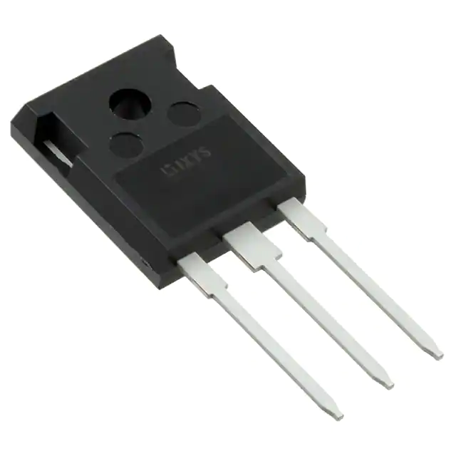
TO-268 (D3) ( IXFT)
EAS
dv/dt
IS ≤ IDM, di/dt ≤ 100 A/µs, VDD ≤ VDSS,
TJ ≤ 150°C, RG = 2 Ω
PD
TC = 25°C
TJ
TJM
150
°C
Tstg
-55 ... +150
°C
300
°C
TL
1.6 mm (0.063 in) from case for 10 s
Md
Mounting torque
Weight
TO-247
TO-268
Symbol
Test Conditions
VDSS
VGS = 0 V, ID = 1 mA
VGS(th)
VDS = VGS, ID = 2.5 mA
IGSS
VGS = ±20 VDC, VDS = 0
IDSS
VDS = 0.8 VDSS
VGS = 0 V
RDS(on)
TO-247 AD (IXFH)
1.13/10
G
G = Gate
S = Source
g
g
Characteristic Values
(TJ = 25°C, unless otherwise specified)
min.
typ.
max.
900
V
Features
z
z
z
z
z
5.0
V
z
±100
nA
TJ = 25°C
TJ = 125°C
50
1
µA
mA
VGS = 10 V, ID = 0.5 ID25
Pulse test, t ≤ 300 µs, duty cycle d ≤ 2 %
1.5
Ω
© 2002 IXYS All rights reserved
D = Drain
TAB = Drain
Nm/lb.in.
6
4
3.0
(TAB)
S
IXYS advanced low Qg process
Low gate charge and capacitances
- easier to drive
- faster switching
International standard packages
Low RDS (on)
Unclamped Inductive Switching (UIS)
rated
Molding epoxies meet UL 94 V-0
flammability classification
Advantages
z
z
z
Easy to mount
Space savings
High power density
DS98645A(12/02)
�IXFH
IXFT
Symbol
Test Conditions
Characteristic Values
(TJ = 25°C, unless otherwise specified)
min. typ. max.
gfs
VDS = 10 V; ID = 0.5 • ID25, pulse test
3
6
S
2200
pF
210
pF
Crss
35
pF
td(on)
15
ns
15
ns
Ciss
Coss
VGS = 0 V, VDS = 25 V, f = 1 MHz
tr
VGS = 10 V, VDS = 0.5 • VDSS, ID = 0.5 • ID25
td(off)
RG = 4.7 Ω (External),
42
ns
tf
13
ns
Qg(on)
56
nC
18
nC
24
Qgs
VGS = 10 V, VDS = 0.5 • VDSS, ID = 0.5 • ID25
Qgd
0.7
RthJC
RthCK
(TO-247)
Source-Drain Diode
Symbol
Test Conditions
IS
VGS = 0 V
ISM
VSD
t rr
QRM
IRM
0.25
1
2
3
Terminals:
1 - Gate
2 - Drain
3 - Source
Tab - Drain
Dim.
Millimeter
Min.
Max.
Inches
Min.
Max.
4.7
2.2
2.2
5.3
2.54
2.6
.185
.087
.059
.209
.102
.098
nC
b
b1
b2
1.0
1.65
2.87
1.4
2.13
3.12
.040
.065
.113
.055
.084
.123
K/W
C
D
E
.4
20.80
15.75
.8
21.46
16.26
.016
.819
.610
.031
.845
.640
e
L
L1
5.20
19.81
5.72
20.32
4.50
0.205
.780
0.225
.800
.177
∅P
Q
3.55
5.89
3.65
6.40
.140
0.232
.144
0.252
R
S
4.32
6.15
5.49
BSC
.170
242
.216
BSC
K/W
7
A
Repetitive; pulse width limited by TJM
28
A
IF = IS, VGS = 0 V,
Pulse test, t ≤ 300 µs, duty cycle d ≤ 2 %
1.5
V
250
ns
µC
A
0.75
5.5
TO-247 AD (IXFH) Outline
A
A1
A2
Characteristic Values
(TJ = 25°C, unless otherwise specified)
min. typ. max.
IF = IS, -di/dt = 100 A/µs, VR = 100 V
7N90Q
7N90Q
TO-268 Outline
Terminals: 1 - Gate
3 - Source
2 - Drain
Tab - Drain
IXYS reserves the right to change limits, test conditions, and dimensions.
IXYS MOSFETs and IGBTs are covered by one or more of the following U.S. patents:
4,835,592
4,850,072
4,881,106
4,931,844
5,017,508
5,034,796
5,049,961
5,063,307
5,187,117
5,237,481
5,486,715
5,381,025
6,306,728B1
�Disclaimer Notice - Information furnished is believed to be accurate and reliable. However, users should independently
evaluate the suitability of and test each product selected for their own applications. Littelfuse products are not designed for,
and may not be used in, all applications. Read complete Disclaimer Notice at www.littelfuse.com/disclaimer-electronics.
�