Preliminary Data Sheet
VDSS
HiPerFET
Power MOSFETs
TM
IXFH8N80 800V
IXFH9N80 800V
ID25
RDS(on)
trr
8A
9A
1.1Ω
0.9Ω
250 ns
250 ns
N-Channel Enhancement Mode
High dv/dt, Low trr, HDMOSTM Family
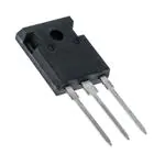
TO-247 AD (IXFH)
Symbol
Test Conditions
Maximum Ratings
VDSS
TJ = 25°C to 150°C
800
V
VDGR
TJ = 25°C to 150°C; RGS = 1 MΩ
800
V
VGS
Continuous
±20
V
VGSM
Transient
±30
V
ID25
TC = 25°C
IDM
TC = 25°C, pulse width limited by TJM
IAR
TC = 25°C
8
9
32
36
8
9
A
A
A
A
A
A
EAR
TC = 25°C
18
mJ
dv/dt
IS ≤ IDM, di/dt ≤ 100 A/µs, VDD ≤ VDSS,
TJ ≤ 150°C, RG = 2 Ω
5
V/ns
PD
TC = 25°C
180
W
8N80
9N80
8N80
9N80
8N80
9N80
-55 ... +150
°C
TJM
150
°C
Tstg
-55 ... +150
°C
TJ
Md
Mounting torque
1.13/10 Nm/lb.in.
Weight
TO-204 = 18 g, TO-247 = 6 g
Maximum lead temperature for soldering
1.6 mm (0.062 in.) from case for 10 s
Symbol
VDSS
VGS(th)
Test Conditions
IDSS
VDS = 0.8 VDSS
VGS = 0 V
RDS(on)
Characteristic Values
(TJ = 25°C, unless otherwise specified)
min. typ.
max.
VDS = VGS, ID = 2.5 mA
VGS(th) temperature coefficient
VGS = ±20 VDC, VDS = 0
800
V
%/K
0.088
2
4.5
-0.257
TJ = 25°C
TJ = 125°C
VGS = 10 V, ID = 0.5 ID25
Pulse test, t ≤ 300 µs, duty cycle δ ≤ 2%
© 1997 IXYS All rights reserved
G
G = Gate
S = Source
8N80
9N80
V
%/K
±100
nA
250
1
µA
mA
1.1
0.9
Ω
Ω
D (TAB)
S
D = Drain
TAB = Drain
*Add suffix letter "S" for surface mountable
package
Features
•
•
•
•
•
VGS = 0 V, ID = 3 mA
VDSS temperature coefficient
IGSS
°C
300
TO-247 SMD*
•
International standard packages
Low RDS (on) HDMOSTM process
Rugged polysilicon gate cell structure
Unclamped Inductive Switching (UIS)
rated
Low package inductance
- easy to drive and to protect
Fast intrinsic Rectifier
Applications
•
•
•
•
•
•
DC-DC converters
Battery chargers
Switched-mode and resonant-mode
power supplies
DC choppers
AC motor control
Temperature and lighting controls
Advantages
•
•
•
Easy to mount with 1 screw (TO-247)
(isolated mounting screw hole)
Space savings
High power density
96527A (8/97)
�IXFH8N80
IXFH9N80
TO-247 AD (IXFH) Outline
Symbol
Test Conditions
Characteristic Values
(TJ = 25°C, unless otherwise specified)
min. typ. max.
gfs
VDS = 10 V; ID = 0.5 ID25, pulse test
4
Ciss
7
S
2600
pF
240
pF
Crss
60
pF
td(on)
35
ns
Coss
VGS = 0 V, VDS = 25 V, f = 1 MHz
tr
VGS = 10 V, VDS = 0.5 VDSS, ID = 0.5 ID25
15
ns
td(off)
RG = 4.7 Ω (External)
70
ns
tf
35
ns
Qg(on)
85 130
nC
15
30
nC
40
70
nC
0.7
K/W
Qgs
VGS = 10 V, VDS = 0.5 VDSS, ID = 0.5 ID25
Qgd
RthJC
RthCK
0.25
K/W
TO-247 SMD Outline
Source-Drain Diode
Characteristic Values
(TJ = 25°C, unless otherwise specified)
min. typ. max.
Symbol
Test Conditions
IS
VGS = 0
8N80
9N80
8
9
A
A
I SM
Repetitive; pulse width limited by TJM
8N80
9N80
32
36
A
A
VSD
IF = IS, VGS = 0 V,
Pulse test, t ≤ 300 µs, duty cycle δ ≤ 2 %
1.5
V
250
400
ns
ns
trr
Q RM
I RM
IF = IS
-di/dt = 100 A/µs,
VR = 100 V
TJ = 25°C
TJ = 125°C
TJ = 25°C
TJ = 125°C
0.5
1.0
µC
µC
TJ = 25°C
TJ = 125°C
7.5
9.0
A
A
IXYS reserves the right to change limits, test conditions, and dimensions.
IXYS MOSFETS and IGBTs are covered by one or more of the following U.S. patents:
4,835,592
4,850,072
4,881,106
4,931,844
1. Gate
2. Drain
3. Source
4. Drain
Dim.
Millimeter
Min.
Max.
Inches
Min. Max.
A
A1
A2
4.83
2.29
1.91
5.21
2.54
2.16
.190
.090
.075
.205
.100
.085
b
b1
1.14
1.91
1.40
2.13
.045
.075
.055
.084
C
D
0.61
20.80
0.80
21.34
.024
.819
.031
.840
E
e
15.75
5.45
16.13
BSC
.620
.215
.635
BSC
L
L1
L2
L3
L4
4.90
2.70
2.10
0.00
1.90
5.10
2.90
2.30
0.10
2.10
.193
.106
.083
.00
.075
.201
.114
.091
.004
.083
ØP
Q
3.55
5.59
3.65
6.20
.140
.220
.144
.244
R
S
4.32
6.15
4.83
BSC
.170
.242
.190
BSC
5,017,508
5,034,796
5,049,961
5,063,307
5,187,117
5,237,481
5,486,715
5,381,025
�IXFH8N80
Figure 1. Output Characteristics at 25OC
��
7
-�
9
2
*6
��� &
IXFH9N80
Figure 2. Output Characteristics at 125OC
��
��9
7
�9
-�
�
9
2
���� &
*6
��9
�9
�
, ���$ P SHUHV
, ���$ P SHUHV
�9
�9
�
�
'
�
�
'
�
�
�
�
�
�
�
�
�
��
�
�
9 '6���9ROW
V
���
��� &
-
9
9
� ���9
���1 RUP DO
L] HG
*6
���1 RUP DOL] HG
��
2
7 �
���
���
�
1
2
�
�
1
2
�
6
'
5
���
5
��
Figure 4. RDS(on) normalized to 15A/25OC vs. TJ
���
���
*6�
���9
���
,
'�
��$
���
���
���
�
�
�
�
�
��
��
��
,'���$ P SHUHV
��
���
���
Figure 6. Admittance Curves
��
��
�
,;)+�1��
�
�
, ���$ P SHUHV
,;)+�1��
�
�
'
7 �
-
R
���� &
�
�
'
7 �
-
�
R
��� &
�
�
���
���
7 -���' HJUHHV�&
Figure 5. Drain Current vs. Case Temperature
, ���$ P SHUHV
��
9 '6���9 RO
W
V
Figure 3. RDS(on) normalized to 15A/25OC vs. ID
6
'
�
���
�
��
��
��
7 &���' HJUHHV�&
© 1997 IXYS All rights reserved
���
���
���
�
�
�
�
�
9 *6���9 ROW
V
�
�
�IXFH8N80
Figure 8. Capacitance Curves
Figure 7. Gate Charge
�����
��
��
9
'6�
R
9
�
�
�
6
*
9
�
����9
���,
��$
���,
��P$
'�
V
OW
IXFH9N80
*�
)
S
�
�
�
H
F
Q
D
W
L
F
D
S
D
&
�
�
&LVV
I�
��0+]
����
&RVV
���
&UVV
�
��
�
�
��
��
��
��
���
�
���
�
��
��
9
*DWH�&KDUJH���Q&
��
'6
��
��
��
��
���9ROWV
Figure10. Forward Bias Safe Operating Area
Figure 9. Forward Voltage Drop of the Intrinsic Diode
��
��
�
V
H
U
H
S
P
$
�
�
�
,
'
10
V
H
U
H
S
�
7
-�
����
2
P
$
�
�
�
&
�
,
7
'
��PV
���
1
7 �
2
-�
&
��� &
���
2
PV
&
����
�
PV
'&
0 .1
�
���
���
���
9
6'
���
���
���
1
10
����9ROWV
100
9
'6�
���
��9ROWV
Figure 11. Transient Thermal Resistance
����
:
�
.
�
�
�
����
&-
�
K
W
�
5
'
���
'
���
'
���
'
����
'
����
'
����
6LQJOH�3XOVH
����
����
��
��
��
��
��
��
��
��
��
��
��
�
��
�
3XOVH�:LGWK���6HFRQGV
IXYS reserves the right to change limits, test conditions, and dimensions.
IXYS MOSFETS and IGBTs are covered by one or more of the following U.S. patents:
4,835,592
4,850,072
4,881,106
4,931,844
5,017,508
5,034,796
5,049,961
5,063,307
5,187,117
5,237,481
5,486,715
5,381,025
�Disclaimer Notice - Information furnished is believed to be accurate and reliable. However, users should independently
evaluate the suitability of and test each product selected for their own applications. Littelfuse products are not designed for,
and may not be used in, all applications. Read complete Disclaimer Notice at www.littelfuse.com/disclaimer-electronics.
�