Advance Technical Information
IXFJ26N50P3
Polar3TM HiperFETTM
Power MOSFET
VDSS
ID25
RDS(on)
= 500V
= 14A
265m
(Electrically Isolated Tab)
N-Channel Enhancement Mode
Avalanche Rated
Fast Intrinsic Rectifier
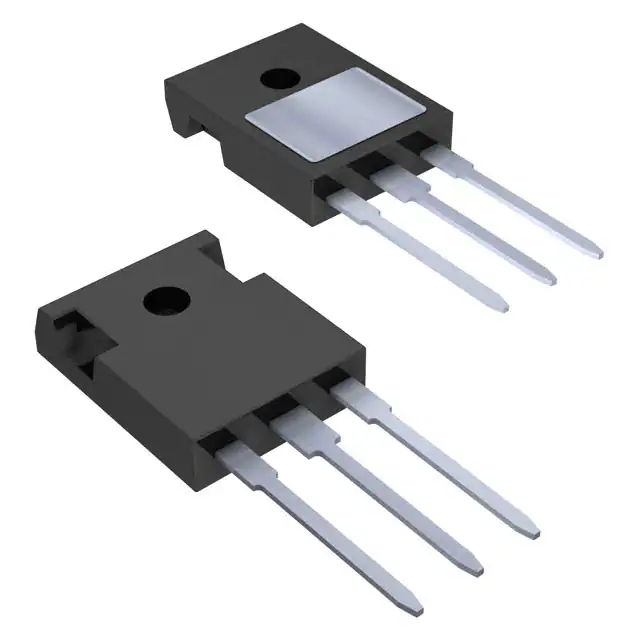
ISO TO-247TM
E153432
Symbol
Test Conditions
Maximum Ratings
VDSS
TJ = 25C to 150C
500
V
VDGR
TJ = 25C to 150C, RGS = 1M
500
V
VGSS
VGSM
Continuous
Transient
30
40
V
V
ID25
TC = 25C
14
A
IDM
TC = 25C, Pulse Width Limited by TJM
78
A
IA
TC = 25C
13
A
EAS
TC = 25C
300
mJ
dv/dt
IS IDM, VDD VDSS, TJ 150°C
35
V/ns
PD
TC = 25C
180
W
G
-55 ... +150
C
TJM
150
C
Tstg
-55 ... +150
C
TJ
TL
TSOLD
Maximum Lead Temperature for Soldering
Plastic Body for 10s
FC
Mounting Torque
VISOL
50/60 Hz, RM, t = 1min
300
260
°C
°C
1.13 / 10
Nm/lb.in
2500
V~
5
g
Weight
BVDSS
VGS = 0V, ID = 1mA
500
VGS(th)
VDS = VGS, ID = 4mA
3.0
IGSS
VGS = 30V, VDS = 0V
IDSS
VDS = VDSS, VGS = 0V
RDS(on)
VGS = 10V, ID = 13A, Note 1
TJ = 125C
© 2014 IXYS CORPORATION, All Rights Reserved
D
= Drain
Features
Silicon Chip on Direct-Copper Bond
(DCB) Substrate
Isolated Mounting Surface
2500V~ Electrical Isolation
Fast Intrinsic Rectifier
Avalanche Rated
Low RDS(ON) and QG
Low Package Inductance
Advantages
Characteristic Values
Min.
Typ.
Max.
Isolated Tab
S
G = Gate
S = Source
Symbol
Test Conditions
(TJ = 25C Unless Otherwise Specified)
D
High Power Density
Easy to Mount
Space Savings
Applications
V
5.0
V
100
nA
25 A
750 A
Switch-Mode and Resonant-Mode
Power Supplies
DC-DC Converters
Laser Drivers
AC and DC Motor Drives
Robotics and Servo Controls
265 m
DS100603(03/14)
�IXFJ26N50P3
Symbol
Test Conditions
(TJ = 25C Unless Otherwise Specified)
gfs
Characteristic Values
Min.
Typ.
Max.
VDS = 20V, ID = 13A, Note 1
14
Ciss
Coss
23
S
2220
pF
280
pF
8
pF
VGS = 0V, VDS = 25V, f = 1MHz
Crss
RGi
Gate Input Resistance
td(on)
Resistive Switching Times
tr
ISO TO-247 (IXFJ) OUTLINE
2.1
21
ns
7
ns
38
ns
5
ns
42
nC
11
nC
Qgd
15
nC
RthJC
RthCS
0.30
td(off)
tf
VGS = 10V, VDS = 0.5 • VDSS, ID = 13A
RG = 3 (External)
Qg(on)
Qgs
VGS = 10V, VDS = 0.5 • VDSS, ID = 13A
PINS:
1 = Gate
2 = Drain
3 = Source
4 = Isolated
0.69 C/W
°C/W
Source-Drain Diode
Symbol
Test Conditions
(TJ = 25C Unless Otherwise Specified)
IS
VGS = 0V
ISM
VSD
trr
IRM
QRM
Note
Characteristic Values
Min.
Typ.
Max.
26
A
Repetitive, Pulse Width Limited by TJM
104
A
IF = IS, VGS = 0V, Note 1
1.4
V
250
ns
IF = 13A, -di/dt = 100A/s
VR = 100V, VGS = 0V
10.2
A
0.9
μC
1. Pulse test, t 300s, duty cycle, d 2%.
ADVANCETECHNICALINFORMATION
The product presented herein is under development. The Technical Specifications offered are
derived from a subjective evaluation of the design, based upon prior knowledge and experience,
and constitute a "considered reflection" of the anticipated result. IXYS reserves the right to
change limits, test conditions, and dimensions without notice.
IXYS Reserves the Right to Change Limits, Test Conditions, and Dimensions.
IXYS MOSFETs and IGBTs are covered
4,835,592
by one or more of the following U.S. patents: 4,860,072
4,881,106
4,931,844
5,017,508
5,034,796
5,049,961
5,063,307
5,187,117
5,237,481
5,381,025
5,486,715
6,162,665
6,259,123 B1
6,306,728 B1
6,404,065 B1
6,534,343
6,583,505
6,683,344
6,727,585
7,005,734 B2
6,710,405 B2 6,759,692
7,063,975 B2
6,710,463
6,771,478 B2 7,071,537
7,157,338B2
�IXFJ26N50P3
Fig. 1. Output Characteristics @ TJ = 25ºC
Fig. 2. Extended Output Characteristics @ TJ = 25ºC
28
VGS = 10V
8V
7V
24
VGS = 10V
8V
50
7V
40
6V
I D - Amperes
I D - Amperes
20
16
12
30
6V
20
8
10
4
5V
5V
0
0
0
1
2
3
4
5
6
7
0
5
10
15
VDS - Volts
25
30
Fig. 4. RDS(on) Normalized to ID = 13A Value vs.
Junction Temperature
Fig. 3. Output Characteristics @ TJ = 125ºC
3.4
28
VGS = 10V
7V
3.0
RDS(on) - Normalized
24
20
6V
I D - Amperes
20
VDS - Volts
16
12
5V
VGS = 10V
2.6
I D = 26A
2.2
1.8
I D = 13A
1.4
8
1.0
4
0.6
4V
0
0.2
0
2
4
6
8
10
12
14
16
-50
-25
0
25
50
75
100
VDS - Volts
TJ - Degrees Centigrade
Fig. 5. RDS(on) Normalized to ID = 13A Value vs.
Drain Current
Fig. 6. Maximum Drain Current vs.
Case Temperature
3.8
125
150
16
VGS = 10V
14
3.4
12
TJ = 125ºC
I D - Amperes
R DS(on) - Normalized
3.0
2.6
2.2
1.8
TJ = 25ºC
10
8
6
4
1.4
2
1.0
0
0.6
-50
0
5
10
15
20
25
30
35
I D - Amperes
© 2014 IXYS CORPORATION, All Rights Reserved
40
45
50
55
-25
0
25
50
75
TC - Degrees Centigrade
100
125
150
�IXFJ26N50P3
Fig. 8. Transconductance
Fig. 7. Input Admittance
45
30
TJ = - 40ºC
40
25
35
15
g f s - Siemens
I D - Amperes
20
TJ = 125ºC
25ºC
- 40ºC
10
25ºC
30
125ºC
25
20
15
10
5
5
0
0
3.0
3.5
4.0
4.5
5.0
5.5
6.0
0
6.5
5
10
15
VGS - Volts
20
25
30
I D - Amperes
Fig. 9. Forward Voltage Drop of Intrinsic Diode
Fig. 10. Gate Charge
10
80
VDS = 250V
9
70
I D = 13A
8
I G = 10mA
60
7
VGS - Volts
I S - Amperes
50
40
30
TJ = 125ºC
5
4
3
TJ = 25ºC
20
6
2
10
1
0
0
0.3
0.4
0.5
0.6
0.7
0.8
0.9
1.0
1.1
0
5
10
VSD - Volts
15
20
25
30
35
40
45
QG - NanoCoulombs
Fig. 12. Forward-Bias Safe Operating Area
Fig. 11. Capacitance
100
10,000
RDS(on) Limit
Ciss
10
1,000
I D - Amperes
Capacitance - PicoFarads
25µs
Coss
100
1
100µs
0.1
10
TJ = 150ºC
TC = 25ºC
Single Pulse
Crss
f = 1 MHz
1
1ms
0.01
0
5
10
15
20
25
30
35
40
VDS - Volts
IXYS Reserves the Right to Change Limits, Test Conditions, and Dimensions.
10
100
VDS - Volts
1,000
�IXFJ26N50P3
Fig. 13. Maximum Transient Thermal Impedance
1
Z (th)JC - ºC / W
0.1
0.01
0.001
0.00001
0.0001
0.001
0.01
0.1
1
10
Pulse Width - Seconds
© 2014 IXYS CORPORATION, All Rights Reserved
IXYS REF: F_26N50P3(W6) 3-20-14-A
�