IXFJ 32N50Q VDSS
HiPerFETTM
Power MOSFETs
ID(cont)
RDS(on)
trr
Q-Class
N-Channel Enhancement Mode
Avalanche Rated
High dv/dt, Low trr, HDMOSTM Family
= 500
= 32
= 0.15
< 250
V
A
W
ns
Preliminary data sheet
Symbol
Test Conditions
Maximum Ratings
VDSS
TJ = 25°C to 150°C
500
V
VDGR
TJ = 25°C to 150°C; RGS = 1 MW
500
V
VGS
Continuous
±20
V
VGSM
Transient
±30
V
ID25
TC = 25°C
32
A
IDM
TC = 25°C, pulse width limited by TJM
128
A
IAR
TC = 25°C
32
A
EAs
TC = 25°C
1.5
J
EAR
TC = 25°C
45
mJ
dv/dt
IS £ IDM, di/dt £ 100 A/ms, VDD £ VDSS,
TJ £ 150°C, RG = 2 W
5
V/ns
PD
TC = 25°C
360
W
-55 ... +150
°C
TJM
150
°C
Tstg
-55 ... +150
°C
300
°C
TJ
TL
1.6 mm (0.062 in.) from case for 10 s
G
é
D
S
G = Gate,
S = Source,
(TAB)
D = Drain,
TAB = Drain
Features
• Low profile, high power package
• Long creep and strike distances
• Easy up-grade path for TO-220
designs
• Low RDS (on) low Qg process
• Rugged polysilicon gate cell structure
• Unclamped Inductive Switching (UIS)
rated
• Low package inductance
- easy to drive and to protect
• Fast intrinsic Rectifier
Applications
Symbol
Test Conditions
VDSS
VGS = 0 V, ID = 250 mA
VGS(th)
VDS = VGS, ID = 4 mA
IGSS
VGS = ±20 VDC, VDS = 0
IDSS
VDS = VDSS
VGS = 0 V
RDS(on)
Characteristic Values
(TJ = 25°C, unless otherwise specified)
min. typ. max.
500
V
•
•
•
•
DC-DC converters
Synchronous rectification
Battery chargers
Switched-mode and resonant-mode
power supplies
DC choppers
AC motor control
Temperature and lighting controls
Low voltage relays
4
V
±100
nA
•
•
•
•
TJ = 25°C
TJ = 125°C
100
1
mA
mA
Advantages
VGS = 10 V, ID = 0.5 ID25
Pulse test, t £ 300 ms, duty cycle d £ 2 %
0.15
W
2
IXYS reserves the right to change limits, test conditions, and dimensions.
© 2000 IXYS All rights reserved
• High power, low profile package
• Space savings
• High power density
98579B (5/31/00)
1-4
�IXFJ 32N50Q
Symbol
Test Conditions
Characteristic Values
(TJ = 25°C, unless otherwise specified)
min. typ. max.
gfs
VDS = 10 V; ID = 0.5 ID25, pulse test
C iss
Coss
VGS = 0 V, VDS = 25 V, f = 1 MHz
C rss
td(on)
18
28
S
3950
pF
640
pF
210
pF
35
ns
tr
VGS = 10 V, VDS = 0.5 • VDSS, ID = 0.5 ID25
42
ns
td(off)
RG = 2 W (External)
75
ns
20
ns
153
nC
26
nC
85
nC
tf
Qg(on)
Qgs
VGS = 10 V, VDS = 0.5 • VDSS, ID = 0.5 ID25
Qgd
RthJC
0.35
RthCK
0.25
Source-Drain Diode
Symbol
Test Conditions
IS
VGS = 0 V
ISM
VSD
t rr
Q rr
IRM
K/W
K/W
Characteristic Values
(TJ = 25°C, unless otherwise specified)
min. typ. max.
32
A
Repetitive;
pulse width limited by TJM
128
A
IF = IS, VGS = 0 V,
Pulse test, t £ 300 ms, duty cycle d £ 2 %
1.5
V
250
IF = IS -di/dt = 100 A/ms, VR = 100 V
© 2000 IXYS All rights reserved
0.75
7.5
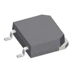
TO-268 Outline
All metal area are
solder plated
1 - gate
2 - drain (collector)
3 - source (emitter)
4 - drain (collector)
Dim.
Inches
Min
Max
Millimeters
Min
Max
A
A1
b
b2
.193
.106
.045
.075
.201
.114
.057
.083
4.90
2.70
1.15
1.90
5.10
2.90
1.45
2.10
C
C2
.016
.057
.026
.063
.040
1.45
.065
1.60
D
D1
E
E1
e
.543
.551
.488
.500
.624
.632
.524
.535
.215 BSC
H
1.365
1.395 34.67 35.43
L
L1
L2
.780
.079
.039
.800
.091
.045
13.80 14.00
12.40 12.70
15.85 16.05
13.30 13.60
5.45 BSC
19.81 20.32
2.00 2.30
1.00 1.15
ns
mC
A
IXYS MOSFETS and IGBTs are covered by one or more of the following U.S. patents:
4,835,592
4,881,106
5,017,508
5,049,961
5,187,117
5,486,715
4,850,072
4,931,844
5,034,796
5,063,307
5,237,481
5,381,025
2-4
�IXFJ 32N50Q
Figure 1. Output Characteristics at 25OC
80
T J = 125 OC
6V
50
40
30
20
30
5V
20
4V
0
0
4
8
12
16
0
20
0
4
8
V DS - Volts
RDS(ON) - Normalized
RDS(ON) - Normalized
V GS = 10V
2.4
Tj=125 0 C
2.0
1.6
Tj=25 0 C
1.2
20
30
40
50
2.4
ID = 32A
2.0
ID = 16A
1.6
1.2
0.8
25
60
50
Figure 5. Drain Current vs. Case Temperature
32
40
ID - Amperes
50
24
16
8
0
25
50
75
T C - Degrees C
© 2000 IXYS All rights reserved
125
150
30
20
100 125 150
0
T J = 25 oC
TJ = 125 oC
10
-25
100
Figure 6. Admittance Curves
40
-50
75
T J - Degrees C
ID - Amperes
0
20
2.8
V GS = 10V
10
16
Figure 4. RDS(on) normalized to 15A/25OC vs. TJ
2.8
0
12
V DS - Volts
Figure 3. RDS(on) normalized to 15A/25OC vs. ID
ID - Amperes
6V
10
5V
10
0.8
V GS = 9V
8V
7V
40
ID - Amperes
60
ID - Amperes
50
V GS =10V
9V
8V
7V
T J = 25 O C
70
Figure 2. Output Characteristics at 125OC
2
3
4
5
6
VGS - Volts
3-4
�IXFJ 32N50Q
Figure 7. Gate Charge
14
10000
Vds=300V
ID=16A
IG=10mA
VGS - Volts
10
F = 1MHz
Ciss
Capacitance - pF
12
Figure 8. Capacitance Curves
8
6
4
Coss
1000
Crss
2
0
0
50
100
150
200
100
250
0
Gate Charge - nC
5
10
15
20
25
VDS - Volts
Figure 9. Forward Voltage Drop of the
Intrinsic Diode
100
VGS= 0V
ID - Amperes
80
60
TJ=125OC
40
20
TJ=25OC
0
0.4
0.6
0.8
1.0
1.2
VSD - Volts
Figure 10. Transient Thermal Resistance
0.40
R(th)JC - K/W
0.20
0.10
0.08
0.06
0.04
0.02
0.01
10-3
10-2
10-1
100
101
Pulse Width - Seconds
© 2000 IXYS All rights reserved
4-4
�