Not for New Designs
VDSS
HiPerFETTM Power MOSFETs
IXFK
IXFK
IXFN
IXFN
N-Channel Enhancement Mode
Avalanche Rated, High dv/dt, Low trr
27N80
25N80
27N80
25N80
800
800
800
800
ID25
V
V
V
V
RDS(on)
27 A
25 A
27 A
25 A
0.30
0.35
0.30
0.35
Ω
Ω
Ω
Ω
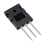
TO-264 AA (IXFK)
Symbol
Test Conditions
Maximum Ratings
IXFK
IXFN
VDSS
TJ = 25°C to 150°C
800
800
V
VDGR
TJ = 25°C to 150°C; RGS = 1 MΩ
800
800
V
VGS
Continuous
±20
±20
V
VGSM
Transient
±30
±30
V
ID25
TC = 25°C, Chip capability
IDM
TC = 25°C, pulse width limited by TJM
TC = 25°C
27N80 27
25N80 25
27N80 108
25N80 100
27N80 14
25N80 13
27
25
108
100
14
13
A
A
A
A
A
A
30
30
mJ
5
5
V/ns
IAR
EAR
TC= 25°C
dv/dt
IS≤ IDM, di/dt ≤ 100 A/µs, VDD ≤ VDSS,
TJ ≤ 150°C, RG = 2 Ω
PD
TC = 25°C
500
520
W
-55 ... +150
°C
TJM
150
°C
Tstg
-55 ... +150
°C
TJ
TL
1.6 mm (0.063 in) from case for 10 s
VISOL
50/60 Hz, RMS
IISOL ≤ 1 mA
Md
Mounting torque
Terminal connection torque
t = 1 min
t=1s
300
-
°C
-
2500
3000
V~
V~
0.9/6
-
Weight
1.5/13 Nm/lb.in.
1.5/13 Nm/lb.in.
10
30
g
D
Test Conditions
Characteristic Values
(TJ = 25°C, unless otherwise specified)
min.
typ.
max.
VDSS
VGS = 0 V, ID = 3 mA
VDSS temperature coefficient
800
VGH(th)
VDS = VGS, ID = 8 mA
VGS(th) temperature coefficient
2
V
%/K
0.096
4.5
V
%/K
±200
nA
-0.214
IGSS
VGS = ±20 VDC, VDS = 0
IDSS
VDS = 0.8 • VDSS
VGS = 0 V
TJ = 25°C
TJ = 125°C
500
2
µA
mA
RDS(on)
VGS = 10 V, ID = 0.5 • ID25
Pulse test, t ≤ 300 µs,
duty cycle d ≤ 2 %
25N80
27N80
0.35
0.30
Ω
Ω
© 2002 IXYS All rights reserved
S
miniBLOC, SOT-227 B (IXFN)
E153432
S
G
D
G
S
S
D
S
G = Gate
S = Source
D = Drain
TAB = Drain
Either Source terminal at miniBLOC can be used
as Main or Kelvin Source
Features
•
•
•
•
•
•
Symbol
(TAB)
G
•
•
International standard packages
JEDEC TO-264 AA, epoxy meet
UL 94 V-0, flammability classification
miniBLOC, with Aluminium nitride
isolation
Low RDS (on) HDMOSTM process
Rugged polysilicon gate cell structure
Unclamped Inductive Switching (UIS)
rated
Low package inductance
Fast intrinsic Rectifier
Applications
•
•
•
•
•
DC-DC converters
Battery chargers
Switched-mode and resonant-mode
power supplies
DC choppers
Temperature and lighting controls
Advantages
•
•
•
Easy to mount
Space savings
High power density
95561D(6/02)
�IXFK 25N80
IXFN 25N80
Symbol
Test Conditions
Characteristic Values
(TJ = 25°C, unless otherwise specified)
min. typ. max.
gfs
VDS = 10 V; ID = 0.5 • ID25, pulse test
28
VGS
= 0 V, VDS = 25 V, f = 1 MHz
Crss
tr
VGS
td(off)
RG = 1 Ω (External),
712 790
pF
146
192 240
pF
= 10 V, VDS = 0.5 • VDSS, ID = 0.5 • ID25
Qgs
30
ns
80
ns
75
ns
40
tf
Qg(on)
320
VGS
120
RthJC
TO-264 AA
RthCK
TO-264 AA
RthJC
miniBLOC, SOT-227 B
RthCK
miniBLOC, SOT-227 B
Source-Drain Diode
ns
350 400
= 10 V, VDS = 0.5 • VDSS, ID = 0.5 • ID25 38
Qgd
pF
630
td(on)
46
nC
56
nC
130 142
nC
0.25
K/W
0.15
K/W
0.24
0.05
K/W
K/W
Characteristic Values
(TJ = 25°C, unless otherwise specified)
min. typ. max.
Symbol
Test Conditions
IS
VGS = 0 V
27N80
25N80
27
25
A
A
ISM
Repetitive;
pulse width limited by TJM
27N80
25N80
108
100
A
A
VSD
IF = 100 A, VGS = 0 V,
Pulse test, t ≤ 300 µs, duty cycle d ≤ 2 %
1.5
V
t rr
IF = IS, -di/dt = 100 A/µs, VR = 100 V T J =25°C
TJ =125°C
T J =25°C
250
400
ns
ns
µC
A
QRM
IRM
TO-264 AA Outline
S
7930 8400 9740
Ciss
Coss
16
IXFK 27N80
IXFN 27N80
2
17
Dim.
Millimeter
Min.
Max.
A
A1
A2
b
b1
b2
c
D
E
e
J
K
L
L1
P
Q
Q1
R
R1
S
T
4.82
5.13
2.54
2.89
2.00
2.10
1.12
1.42
2.39
2.69
2.90
3.09
0.53
0.83
25.91
26.16
19.81
19.96
5.46 BSC
0.00
0.25
0.00
0.25
20.32
20.83
2.29
2.59
3.17
3.66
6.07
6.27
8.38
8.69
3.81
4.32
1.78
2.29
6.04
6.30
1.57
1.83
Min.
Inches
Max.
.190
.202
.100
.114
.079
.083
.044
.056
.094
.106
.114
.122
.021
.033
1.020
1.030
.780
.786
.215 BSC
.000
.010
.000
.010
.800
.820
.090
.102
.125
.144
.239
.247
.330
.342
.150
.170
.070
.090
.238
.248
.062
.072
miniBLOC, SOT-227 B
M4 screws (4x) supplied
Dim.
Millimeter
Min.
Max.
Inches
Min.
Max.
A
B
31.50
7.80
31.88
8.20
1.240
0.307
1.255
0.323
C
D
4.09
4.09
4.29
4.29
0.161
0.161
0.169
0.169
E
F
4.09
14.91
4.29
15.11
0.161
0.587
0.169
0.595
G
H
30.12
38.00
30.30
38.23
1.186
1.496
1.193
1.505
J
K
11.68
8.92
12.22
9.60
0.460
0.351
0.481
0.378
L
M
0.76
12.60
0.84
12.85
0.030
0.496
0.033
0.506
N
O
25.15
1.98
25.42
2.13
0.990
0.078
1.001
0.084
P
Q
4.95
26.54
5.97
26.90
0.195
1.045
0.235
1.059
R
S
3.94
4.72
4.42
4.85
0.155
0.186
0.174
0.191
T
U
24.59
-0.05
25.07
0.1
0.968
-0.002
0.987
0.004
IXYS reserves the right to change limits, test conditions, and dimensions.
IXYS MOSFETs and IGBTs are covered by one or more of the following U.S. patents:
4,835,592
4,850,072
4,881,106
4,931,844
5,017,508
5,034,796
5,049,961
5,063,307
5,187,117
5,237,481
5,486,715
5,381,025
6,306,728B1
�IXFK 25N80
IXFN 25N80
40
40
TJ = 25 C
TJ = 125OC
VGS = 9V
8V
7V
6V
30
VGS = 9V
8V
7V
6V
30
5V
20
ID - Amperes
O
ID - Amperes
IXFK 27N80
IXFN 27N80
5V
20
10
10
4V
4V
0
0
0
2
4
6
8
10
0
4
8
2.6
2.6
2.2
2.4
TJ = 125OC
RDS(ON) - Normalized
VGS = 10V
2.4
RDS(ON) - Normalized
20
Figure 2. Output Characteristics at 125OC
Figure 1. Output Characteristics at 25OC
2.0
1.8
1.6
1.4
TJ = 25OC
1.2
VGS = 10V
2.2
2.0
ID = 27A
1.8
1.6
ID = 13.5A
1.4
1.2
1.0
0
10
20
30
40
1.0
25
50
50
ID - Amperes
100
125
150
Figure 4. RDS(on) normalized to 0.5 ID25 value vs. TJ
30
30
25
25
IXFN27N80
IXF_25N80
ID - Amperes
20
IXFK27N80
15
10
5
0
-50
75
TJ - Degrees C
Figure 3. RDS(on) normalized to 0.5 ID25 value
vs. ID
ID - Amperes
16
VDS - Volts
VDS - Volts
0.8
12
20
15
TJ = 125oC
10
TJ = 25oC
5
-25
0
25
50
75
100 125 150
TC - Degrees C
Figure 5. Drain Current vs. Case Temperature
© 2002 IXYS All rights reserved
0
2
3
4
5
VGS - Volts
Figure 6. Admittance Curves
6
7
�IXFK 25N80
IXFN 25N80
12
10000
Ciss
8
Capacitance - pF
V
= 400V
Vds=300V
DS
ID=30A
= 27A
= 1mA
IG=10mA
10
VGS - Volts
IXFK 27N80
IXFN 27N80
6
4
f = 1MHz
Coss
1000
Crss
2
0
0
100
200
300
400
100
500
0
5
Gate Charge - nC
10
15
20
25
30
35
40
VDS - Volts
Figure 7. Gate Charge
Figure 8. Capacitance Curves
100
ID - Amperes
80
60
TJ = 125OC
40
TJ = 25OC
20
0
0.2
0.4
0.6
0.8
1.0
1.2
1.4
VSD - Volts
Figure 9. Forward Voltage Drop of the Intrinsic Diode
1
R(th)JC - K/W
D=0.5
0.1
D=0.2
D=0.1
D=0.05
D = Duty Cycle
0.01 D=0.02
D=0.01
Single pulse
0.001
0.0001
0.001
0.01
0.1
1
10
Pulse Width - Seconds
Figure 10. Transient Thermal Resistance
IXYS reserves the right to change limits, test conditions, and dimensions.
IXYS MOSFETs and IGBTs are covered by one or more of the following U.S. patents:
4,835,592
4,850,072
4,881,106
4,931,844
5,017,508
5,034,796
5,049,961
5,063,307
5,187,117
5,237,481
5,486,715
5,381,025
6,306,728B1
�Disclaimer Notice - Information furnished is believed to be accurate and reliable. However, users should independently
evaluate the suitability of and test each product selected for their own applications. Littelfuse products are not designed for,
and may not be used in, all applications. Read complete Disclaimer Notice at www.littelfuse.com/disclaimer-electronics.
�