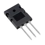
HiPerFETTM
Power MOSFETs
IXFK33N50
IXFX35N50
VDSS
ID25
33A
35A
500V
N-Channel Enhancement Mode
Avalanche Rated
High dv/dt, Low trr
RDS(on)
160m
150m
TO-264 (IXFK)
Symbol
Test Conditions
VDSS
VDGR
TJ = 25C to 150C
TJ = 25C to 150C, RGS = 1M
500
500
V
V
VGSS
VGSM
Continuous
Transient
20
30
V
V
ID25
TC = 25C
IDM
TC = 25C, Pulse Width Limited by TJM
33
35
132
140
A
A
A
A
33
2.5
A
J
5
V/ns
416
W
-55 ... +150
150
-55 ... +150
C
C
C
300
260
°C
°C
1.13/10
Nm/lb.in
20..120 /4.5..27
N/lb
10
6
g
g
G
D
S
Maximum Ratings
IA
EAS
TC = 25C
TC = 25C
dv/dt
IS IDM, VDD VDSS, TJ 150C
PD
TC = 25C
33N50
35N50
33N50
35N50
TJ
TJM
Tstg
TL
TSOLD
Maximum Lead Temperature for Soldering
1.6 mm (0.062in.) from Case for 10s
Md
Mounting Torque (TO-264)
FC
Mounting Force
Weight
TO-264
PLUS247
(PLUS247)
Tab
PLUS247 (IXFX)
G
D
Tab
S
G = Gate
S = Source
D = Drain
Tab = Drain
Features
International Standard Packages
Avalanche Rated
Low Intrinsic Gate Resistance
Low Package Inductance
Fast Intrinsic Rectifier
Molding epoxies meet UL 94 V-0
flammability classification
Low RDS (on) HDMOSTM process
Advantages
Symbol
Test Conditions
(TJ = 25C Unless Otherwise Specified)
Characteristic Values
Min.
Typ.
Max.
BVDSS
VGS = 0V, ID = 1mA
VDSS Temperature Coefficient
500
VGS(th)
VDS = VGS, ID = 4mA
VGS(th) Temperature Coefficient
2.0
IGSS
VGS = 20V, VDS = 0V
IDSS
VDS = 0.8 • VDSS, VGS = 0V
RDS(on)
VGS = 10V, ID = 0.5 • IDSS, Note 1
V
%/K
0.102
4.5
-0.206
200
V
%/K
nA
200 A
2 mA
TJ = 125C
© 2013 IXYS CORPORATION, All Rights Reserved
33N50
35N50
160 m
150 m
High Power Density
Easy to Mount
Space Savings
Applications
DC-DC Converters
Battery Chargers
Synchronous rectification
Switch-Mode and Resonant-Mode
Power Supplies
DC Choppers
Temperature and Lighting Controls
DS97517E(9/13)
�IXFK33N50
IXFX35N50
Symbol
Test Conditions
(TJ = 25C, Unless Otherwise Specified)
gfs
VDS = 10V, ID = 0.5 • IDSS, Note 1
Ciss
Coss
VGS = 0V, VDS = 25V, f = 1MHz
Crss
td(on)
tr
td(off)
tf
Resistive Switching Times
VGS = 10V, VDS = 0.5 • VDSS, ID = 0.5 • IDSS
RG = 1 (External)
Qg(on)
Qgs
Characteristic Values
Min.
Typ.
Max.
18
28
S
5200
5700
nF
640
750
pF
240
310
pF
35
42
110
23
45
50
140
35
ns
ns
ns
ns
227
nC
29
nC
110
nC
VGS = 10V, VDS = 0.5 • VDSS, ID = 0.5 • IDSS
Qgd
TO-264 Outline
RthJC
PINS:
1 - Gate
2,4 - Drain
3 - Source
0.30C/W
RthCS
0.15
C/W
Source-Drain Diode
Symbol
Test Conditions
(TJ = 25C, Unless Otherwise Specified)
IS
VGS = 0V
ISM
Characteristic Values
Min. Typ.
Max.
33
A
Repetitive, Pulse Width Limited by TJM
132
A
VSD
IF = IS, VGS = 0V, Note 1
1.5
V
trr
IRM
IF = IS, VGS = 0V
QRM
Note
-di/dt = 100A/s
VR = 100V
1. Pulse test, t 300s, duty cycle, d 2%.
IXYS Reserves the Right to Change Limits, Test Conditions, and Dimensions.
7
250 ns
A
750
nC
PLUS247TM Outline
PINS:
1 - Gate
2,4 - Drain
3 - Source
�Disclaimer Notice - Information furnished is believed to be accurate and reliable. However, users should independently
evaluate the suitability of and test each product selected for their own applications. Littelfuse products are not designed for,
and may not be used in, all applications. Read complete Disclaimer Notice at www.littelfuse.com/disclaimer-electronics.
�
很抱歉,暂时无法提供与“IXFK33N50”相匹配的价格&库存,您可以联系我们找货
免费人工找货