HiPerFETTM
Power MOSFETs
IXFX 44N60
IXFK 44N60
VDSS
ID25
RDS(on)
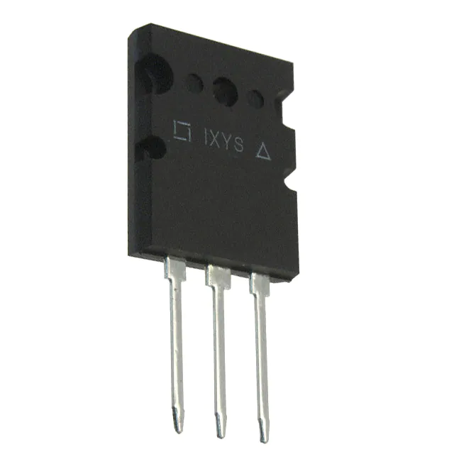
Single MOSFET Die
trr £ 250 ns
Symbol
Test Conditions
VDSS
VDGR
T J = 25°C to 150°C
T J = 25°C to 150°C; RGS = 1 MW
600
600
V
V
VGS
VGSM
Continuous
Transient
±20
±30
V
V
ID25
IDM
IAR
TC = 25°C
TC = 25°C, pulse width limited by TJM
TC = 25°C
44
176
44
A
A
A
EAR
EAS
TC = 25°C
TC = 25°C
60
3
mJ
J
Maximum Ratings
dv/dt
IS £ IDM, di/dt £ 100 A/ms, VDD £ VDSS
T J £ 150°C, RG = 2 W
PD
TC = 25°C
5
V/ns
560
W
TJ
-55 ... +150
°C
TJM
Tstg
150
-55 ... +150
°C
°C
300
°C
TL
1.6 mm (0.063 in.) from case for 10 s
Md
Mounting torque
Weight
TO-264
0.4/6
PLUS 247
TO-264
Nm/lb.in.
6
10
g
g
Symbol
Test Conditions
VDSS
VGS = 0 V, ID = 3mA
600
V
VGS(th)
VDS = VGS, ID = 8mA
2.5
4.5 V
IGSS
VGS = ±20 V, VDS = 0
IDSS
VDS = VDSS
VGS = 0 V
RDS(on)
VGS = 10 V, ID = 0.5 • ID25
Note 1
Characteristic Values
(TJ = 25°C, unless otherwise specified)
min. typ. max.
PLUS 247TM (IXFX)
G
(TAB)
D
TO-264 AA (IXFK)
G
D
G = Gate
S = Source
(TAB)
S
D = Drain
TAB = Drain
Features
• International standard packages
• Low RDS (on) HDMOSTM process
• Rugged polysilicon gate cell structure
• Unclamped Inductive Switching (UIS)
rated
• Low package inductance
- easy to drive and to protect
• Fast intrinsic rectifier
Applications
• DC-DC converters
• Battery chargers
• Switched-mode and resonant-mode
power supplies
• DC choppers
• AC motor control
• Temperature and lighting controls
±100 nA
TJ = 25°C
TJ = 125°C
IXYS reserves the right to change limits, test conditions, and dimensions.
© 2000 IXYS All rights reserved
= 600 V
=
44 A
= 130 mW
100 mA
2 mA
130 mW
Advantages
• PLUS 247TM package for clip or spring
mounting
• Space savings
• High power density
98611B (7/00)
1-4
�IXFK 44N60
IXFX 44N60
Symbol
Test Conditions
gfs
VDS = 10 V; ID = 0.5 • ID25
Characteristic Values
(TJ = 25°C, unless otherwise specified)
min. typ. max.
Note 1
Ciss
Coss
VGS = 0 V, VDS = 25 V, f = 1 MHz
Crss
td(on)
tr
VGS = 10 V, VDS = 0.5 • VDSS, ID = 0.5 • ID25
td(off)
RG = 1 W (External),
tf
Qg(on)
Qgs
VGS = 10 V, VDS = 0.5 • VDSS, ID = 0.5 • ID25
Qgd
30
45
S
8900
pF
1000
pF
330
pF
40
ns
50
ns
100
ns
40
ns
330
nC
60
nC
65
nC
RthJC
0.22
0.15
RthCK
Source-Drain Diode
Symbol
Test Conditions
IS
VGS = 0 V
ISM
VSD
K/W
Characteristic Values
(TJ = 25°C, unless otherwise specified)
min. typ. max.
44
A
Repetitive;
pulse width limited by TJM
176
A
IF = IS, VGS = 0 V, Note 1
1.3
V
250
ns
t rr
QRM
K/W
IF = 50A,-di/dt = 100 A/ms, VR = 100 V
IRM
1.4
mC
8
A
PLUS247TM (IXFX) Outline
Dim.
A
A1
A2
b
b1
b2
C
D
E
e
L
L1
Q
R
Millimeter
Min. Max.
4.83
5.21
2.29
2.54
1.91
2.16
1.14
1.40
1.91
2.13
2.92
3.12
0.61
0.80
20.80 21.34
15.75 16.13
5.45 BSC
19.81 20.32
3.81
4.32
5.59
6.20
4.32
4.83
Inches
Min. Max.
.190 .205
.090 .100
.075 .085
.045 .055
.075 .084
.115 .123
.024 .031
.819 .840
.620 .635
.215 BSC
.780 .800
.150 .170
.220 .244
.170 .190
TO-264 AA (IXFK) Outline
Note: 1. Pulse test, t £ 300 ms, duty cycle d £ 2 %
Dim.
A
A1
A2
b
b1
b2
c
D
E
e
J
K
L
L1
P
Q
Q1
R
R1
S
T
© 2000 IXYS All rights reserved
Millimeter
Min.
Max.
4.82
2.54
2.00
1.12
2.39
2.90
0.53
25.91
19.81
5.46
0.00
0.00
20.32
2.29
3.17
6.07
8.38
3.81
1.78
6.04
1.57
IXYS MOSFETS and IGBTs are covered by one or more of the following U.S. patents:
4,835,592
4,881,106
5,017,508
5,049,961
5,187,117
5,486,715
4,850,072
4,931,844
5,034,796
5,063,307
5,237,481
5,381,025
5.13
2.89
2.10
1.42
2.69
3.09
0.83
26.16
19.96
BSC
0.25
0.25
20.83
2.59
3.66
6.27
8.69
4.32
2.29
6.30
1.83
Inches
Min.
Max.
.190
.202
.100
.114
.079
.083
.044
.056
.094
.106
.114
.122
.021
.033
1.020
1.030
.780
.786
.215 BSC
.000
.010
.000
.010
.800
.820
.090
.102
.125
.144
.239
.247
.330
.342
.150
.170
.070
.090
.238
.248
.062
.072
2-4
�IXFK 44N60
IXFX 44N60
Figure 1. Output Characteristics at 25OC
Figure 2. Output Characteristics at 125OC
80
100
O
TJ = 25 C
60
60
ID - Amperes
ID - Amperes
80
5V
40
5V
40
0
0
0
4
8
12
16
20
0
24
4
8
12
16
20
24
VDS - Volts
VDS - Volts
Figure 3. RDS(on) normalized to 15A/25OC vs. ID
Figure 4. RDS(on) normalized to 15A/25OC vs. TJ
2.4
2.4
VGS = 10V
VGS = 10V
TJ = 125OC
RDS(ON) - Normalized
RDS(ON) - Normalized
6V
20
20
2.0
1.6
TJ = 25OC
1.2
0.8
0
20
40
60
80
2.0
ID = 44A
1.6
ID = 22A
1.2
0.8
25
100
50
ID - Amperes
75
100
Figure 5. Drain Current vs. Case Temperature
Figure 6. Admittance Curves
60
60
50
50
40
30
20
10
150
TJ = 125oC
40
30
TJ = 25oC
20
10
0
-50 -25
125
TJ - Degrees C
ID - Amperes
ID - Amperes
VGS = 10V
9V
8V
7V
TJ = 125OC
VGS = 10V
9V
8V
7V
6V
0
25
50
75
TC - Degrees C
© 2000 IXYS All rights reserved
100 125 150
0
3.0
3.5
4.0
4.5
5.0
5.5
VGS - Volts
3-4
�IXFK 44N60
IXFX 44N60
Figure 7. Gate Charge
Figure 8. Capacitance Curves
12
10000
Capacitance - pF
8
VGS - Volts
Ciss
VDS = 300V
ID = 30A
IG = 10mA
10
6
4
Coss
1000
Crss
2
0
f = 1MHz
0
50 100 150 200 250 300 350 400
100
0
5
10
15
Gate Charge - nC
20
25
30
35
40
VDS - Volts
Figure 9. Forward Voltage Drop of the Intrinsic Diode
100
ID - Amperes
80
TJ = 125OC
60
40
TJ = 25OC
20
0
0.2
0.4
0.6
0.8
1.0
1.2
VSD - Volts
Figure 10. Transient Thermal Resistance
R(th)JC - K/W
1.00
0.10
0.01
0.00
10-4
10-3
10-2
10-1
100
101
Pulse Width - Seconds
© 2000 IXYS All rights reserved
4-4
�Disclaimer Notice - Information furnished is believed to be accurate and reliable. However, users should independently
evaluate the suitability of and test each product selected for their own applications. Littelfuse products are not designed for,
and may not be used in, all applications.Read complete Disclaimer Notice at www.littelfuse.com/disclaimer-electronics.
�