IXFN 120N20
HiPerFETTM
Power MOSFETs
VDSS
ID25
= 200 V
= 120 A
Ω
=
17 mΩ
Single MOSFET Die
RDS(on)
N-Channel Enhancement Mode
Avalanche Rated, High dv/dt, Low trr
trr ≤ 250 ns
Maximum Ratings
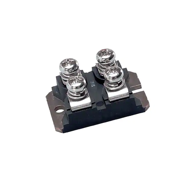
miniBLOC, SOT-227 B (IXFN)
E153432
Symbol
Test Conditions
VDSS
VDGR
TJ = 25°C to 150°C
TJ = 25°C to 150°C; RGS = 1 MΩ
200
200
V
V
VGS
VGSM
Continuous
Transient
±20
±30
V
V
ID25
IDM
IAR
TC = 25°C
TC = 25°C, pulse width limited by TJM
TC = 25°C
120
480
120
A
A
A
EAR
EAS
TC = 25°C
TC = 25°C
64
3
mJ
J
dv/dt
IS ≤ IDM, di/dt ≤ 100 A/µs, VDD ≤ VDSS
TJ ≤ 150°C, RG = 2 Ω
5
V/ns
PD
TC = 25°C
600
W
TJ
-55 ... +150
°C
Features
TJM
Tstg
150
-55 ... +150
°C
°C
-
°C
2500
3000
V~
V~
• Encapsulating epoxy meets
UL 94 V-0, flammability classification
• International standard package
• miniBLOC, with Aluminium nitride
isolation
• Low RDS (on) HDMOSTM process
• Rugged polysilicon gate cell structure
• Unclamped Inductive Switching (UIS)
rated
• Low package inductance
• Fast intrinsic Rectifier
TL
1.6 mm (0.063 in.) from case for 10 s
VISOL
50/60 Hz, RMS
IISOL ≤ 1 mA
Md
Mounting torque
Terminal connection torque
t = 1 min
t=1s
1.5/13 Nm/lb.in.
1.5/13 Nm/lb.in.
Weight
30
g
S
G
S
D
G = Gate
S = Source
D = Drain
Either Source terminal at miniBLOC can be used
as Main or Kelvin Source
Applications
Symbol
Test Conditions
VDSS
VGS = 0 V, ID = 3mA
200
VGS(th)
VDS = VGS, ID = 8mA
2
IGSS
VGS = ±20 V, VDS = 0
IDSS
VDS = VDSS
VGS = 0 V
RDS(on)
VGS = 10 V, ID = 0.5 • ID25
Note 1
© 2003 IXYS All rights reserved
Characteristic Values
(TJ = 25°C, unless otherwise specified)
min. typ. max.
V
4 V
±200 nA
TJ = 25°C
TJ = 125°C
100 µA
2 mA
17 mΩ
• DC-DC converters
• Battery chargers
• Switched-mode and resonant-mode
power supplies
• DC choppers
• Temperature and lighting controls
• Low voltage relays
Advantages
• Easy to mount
• Space savings
• High power density
DS96538D(03/03)
�IXFN 120N20
Symbol
Test Conditions
Characteristic Values
(TJ = 25°C, unless otherwise specified)
min. typ. max.
gfs
VDS = 10 V; ID = 0.5 • ID25
Note 1
40
Ciss
Coss
VGS = 0 V, VDS = 25 V, f = 1 MHz
77
S
9100
pF
2200
pF
Crss
1000
pF
td(on)
42
ns
55
ns
110
ns
40
ns
tr
VGS = 10 V, VDS = 0.5 • VDSS, ID = 0.5 • ID25
td(off)
RG = 1 Ω (External),
tf
Qg(on)
Qgs
Max.
A
B
31.50
7.80
31.88
8.20
1.240
0.307
1.255
0.323
C
D
4.09
4.09
4.29
4.29
0.161
0.161
0.169
0.169
160
nC
E
F
4.09
14.91
4.29
15.11
0.161
0.587
0.169
0.595
G
H
30.12
38.00
30.30
38.23
1.186
1.496
1.193
1.505
J
K
11.68
8.92
12.22
9.60
0.460
0.351
0.481
0.378
L
M
0.76
12.60
0.84
12.85
0.030
0.496
0.033
0.506
N
O
25.15
1.98
25.42
2.13
0.990
0.078
1.001
0.084
P
Q
4.95
26.54
5.97
26.90
0.195
1.045
0.235
1.059
R
S
3.94
4.72
4.42
4.85
0.155
0.186
0.174
0.191
T
U
24.59
-0.05
25.07
0.1
0.968
-0.002
0.987
0.004
0.05
K/W
K/W
Characteristic Values
(TJ = 25°C, unless otherwise specified)
min. typ. max.
Test Conditions
IS
VGS = 0 V
120
A
ISM
Repetitive;
pulse width limited by TJM
480
A
VSD
IF = IS, VGS = 0 V, Note 1
1.5
V
250
ns
trr
IF = 50A,-di/dt = 100 A/µs, VR = 100 V
Inches
Min.
nC
Symbol
QRM
Millimeter
Min.
Max.
50
0.22
Source-Drain Diode
Dim.
nC
RthJC
RthCK
M4 screws (4x) supplied
360
VGS = 10 V, VDS = 0.5 • VDSS, ID = 0.5 • ID25
Qgd
miniBLOC, SOT-227 B
1.1
µC
13
A
IRM
Note: 1. Pulse test, t ≤ 300 µs, duty cycle d ≤ 2 %
IXYS reserves the right to change limits, test conditions, and dimensions.
IXYS MOSFETS and IGBTs are covered by one or more of the following U.S. patents:
4,835,592
4,850,072
4,881,106
4,931,844
5,017,508
5,034,796
5,049,961
5,063,307
5,187,117
5,237,481
5,486,715
5,381,025
6,306,728B1
�IXFN 120N20
Fig. 2. Extended Output Characteristics
Fig. 1. Output Characteristics
@ 25 deg. C
@ 25 Deg. C
120
180
VGS = 10V
9V
8V
7V
80
VGS = 10V
9V
8V
150
6V
ID - Amperes
ID - Amperes
100
60
5V
40
20
120
6V
90
60
5V
30
0
0
0
0.5
1
1.5
2
2.5
3
0
1
2
V DS - Volts
4
5
Fig. 4. R DS(on) Norm alized to I D25 Value vs.
Junction Temperature
@ 125 Deg. C
120
2.5
VGS = 10V
9V
8V
7V
80
VGS = 10V
2.2
RDS(on) - Normalized
100
ID - Amperes
3
V DS - Volts
Fig. 3. Output Characteristics
6V
60
40
5V
20
1.9
1.6
ID = 120A
1.3
ID = 60A
1
0.7
0.4
0
0
1
2
3
4
-50
5
-25
V DS - Volts
0
25
50
75
100
125
150
TJ - Degrees Centigrade
Fig. 5. R DS(on) Norm alized to I D25
Fig. 6. Drain Current vs. Case
Value vs. I D
Tem perature
140
2.2
VGS = 10V
120
1.9
T J = 125ºC
100
ID - Amperes
RDS(on) - Normalized
7V
1.6
1.3
T J = 25ºC
80
60
40
1
20
0.7
0
0
30
60
90
120
ID - Amperes
© 2003 IXYS All rights reserved
150
180
-50
-25
0
25
50
75
100
TC - Degrees Centigrade
125
150
�IXFN 120N20
Fig. 8. Transconductance
Fig. 7. Input Adm ittance
120
150
Gfs - Siemens
ID - Amperes
T J = 25ºC
100
120
90
T J = -40ºC
25ºC
125ºC
60
80
60
40
30
20
0
0
3
3.5
4
4.5
5
5.5
6
6.5
0
30
60
V GS - Volts
Fig. 9. Source Current vs. Source-To-Drain
200
10
160
8
VGS - Volts
IS - Amperes
120
150
180
250
300
Fig. 10. Gate Charge
Voltage
120
T J = 125ºC
80
90
ID - Amperes
VDS = 100V
ID = 60A
IG = 10mA
6
4
T J = 25ºC
40
2
0
0
0.4
0.55
0.7
0.85
1
1.15
1.3
0
V SD - Volts
50
100
150
200
QG - nanoCoulombs
Fig. 12. Maxim um Transient Therm al
Fig. 11. Capacitance
Resistance
1
10000
f = 1M Hz
R(th)JC - (ºC/W)
Capacitance - pF
C iss
C oss
1000
C rss
100
0.1
0.01
0
5
10
15
20
25
30
35
40
1
V DS - Volts
10
100
1000
Pulse Width - milliseconds
IXYS reserves the right to change limits, test conditions, and dimensions.
IXYS MOSFETS and IGBTs are covered by one or more of the following U.S. patents:
4,835,592
4,850,072
4,881,106
4,931,844
5,017,508
5,034,796
5,049,961
5,063,307
5,187,117
5,237,481
5,486,715
5,381,025
6,306,728B1
�Disclaimer Notice - Information furnished is believed to be accurate and reliable. However, users should independently
evaluate the suitability of and test each product selected for their own applications. Littelfuse products are not designed for,
and may not be used in, all applications. Read complete Disclaimer Notice at www.littelfuse.com/disclaimer-electronics.
�