HiPerFETTM Power MOSFETs
Single Die MOSFET
IXFN25N90
IXFN26N90
VDSS
ID25
RDS(on)
900V
25A
900V
26A
330mΩ
Ω
300mΩ
Ω
N-Channel Enhancement Mode
Avalanche Rated,High dv/dt, Low trr
Fast Intrinsic Diode
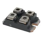
miniBLOC, SOT-227
E153432
Symbol
Test Conditions
Maximum Ratings
VDSS
TJ = 25°C to 150°C
900
V
VDGR
TJ = 25°C to 150°C, RGS = 1MΩ
900
V
VGSS
Continuous
± 20
V
VGSM
Transient
± 30
V
ID25
IDM
ID25
IDM
TC
TC
TC
TC
= 25°C
= 25°C, pulse width limited by TJM
= 25°C
= 25°C, pulse width limited by TJM
25N90
25N90
26N90
26N90
25
100
26
104
A
A
A
A
IAR
IAR
EAR
EAS
TC
TC
TC
TC
= 25°C
= 25°C
= 25°C
= 25°C
25N90
26N90
25
26
64
3
A
A
mJ
J
dV/dt
IS ≤ IDM, VDD ≤ VDSS, TJ ≤ 150°C
5
V/ns
PD
TC = 25°C
600
W
Features
-55 ... +150
°C
z
TJ
S
G
S
D
G = Gate
S = Source
Either Source terminal S can be used as the
Source terminal or the Kelvin Source (gate
return) terminal.
z
TJM
150
°C
Tstg
-55 ... +150
°C
z
300
°C
z
2500
3000
V~
V~
1.5/13
1.3/11.5
Nm/lb.in.
Nm/lb.in.
30
g
TL
1.6mm (0.062 in.) from case for 10s
VISOL
50/60 Hz, RMS
IISOL ≤ 1mA
Md
Mounting torque
Terminal connection torque
z
t = 1min
t = 1s
Weight
D = Drain
z
International standard package
miniBLOC, with Aluminium nitride
isolation
Low RDS(ON) HDMOSTM process
Avalanche Rated
Low package inductance
Fast intrinsic diode
Advantages
z
z
Low gate drive requirement
High power density
Applications:
Symbol
Test Conditions
Characteristic Values
(TJ = 25°C unless otherwise specified)
Min. Typ. Max.
BVDSS
VGS = 0V, ID = 3mA
900
VGS(th)
VDS = VGS, ID = 8mA
3.0
IGSS
VGS = ± 20V, VDS = 0V
IDSS
VDS = 0.8 • VDSS
VGS = 0V
RDS(on)
VGS = 10V, ID = 0.5 • ID25, Note 1
V
z
z
z
z
V
± 200
nA
z
100 μA
2 mA
TJ = 125°C
© 2008 IXYS CORPORATION, All rights reserved
5.0
Switched-mode and resonant-mode
power supplies
DC-DC Converters
Battery chargers
DC choppers
Temperature & lighting controls
25N90
26N90
330 mΩ
300 mΩ
DS97526F(12/08)
�IXFN25N90
IXFN26N90
Symbol
Test Conditions
(TJ = 25°C unless otherwise specified)
Characteristic Values
Min.
Typ.
Max.
gfs
18
VDS = 10V, ID = 0.5 • IDSS, Note 1
Ciss
Coss
VGS = 0V, VDS = 25V, f = 1MHz
Crss
td(on)
Resistive Switching Times
tr
VGS = 10V, VDS = 0.5 • VDSS, ID = 0.5 • IDSS
td(off)
RG = 1Ω (External)
S
8.7
10.8
nF
800
1000
pF
300
375
pF
60
tf
Qg(on)
Qgs
28
VGS = 10V, VDS = 0.5 • VDSS, ID = 0.5 • IDSS
Qgd
SOT-227B Outline
ns
35
ns
130
ns
24
ns
240
nC
56
nC
107
nC
0.21 °C/W
RthJC
RthCS
0.05
Source-Drain Diode
TJ = 25°C unless otherwise specified)
°C/W
Characteristic Values
Min.
Typ.
Max.
IS
VGS = 0V
25N90
26N90
25
26
A
A
ISM
Repetitive, pulse width limited by TJM
25N90
26N90
100
104
A
A
VSD
IF = IS, VGS = 0V, Note 1
1.5
V
250
ns
trr
QRM
IRM
IF = IS, -di/dt = 100A/μs
VR = 100V
1.4
μC
10
A
Note 1: Pulse test, t ≤ 300μs; duty cycle, d ≤ 2%.
IXYS reserves the right to change limits, test conditions, and dimensions.
IXYS MOSFETs and IGBTs are covered
4,835,592
by one or more of the following U.S. patents: 4,850,072
4,881,106
4,931,844
5,017,508
5,034,796
5,049,961
5,063,307
5,187,117
5,237,481
5,381,025
5,486,715
6,162,665
6,259,123 B1
6,306,728 B1
6,404,065 B1
6,534,343
6,583,505
6,683,344
6,727,585
7,005,734 B2
6,710,405 B2 6,759,692
7,063,975 B2
6,710,463
6,771,478 B2 7,071,537
7,157,338B2
�IXFN25N90
IXFN26N90
Figure 1. Output Characteristics at 25OC
Figure 2. Extended Output Characteristics at 125OC
50
20
T J = 25°C V GS = 9V
8V
6V
ID - Amperes
ID - Amperes
40
7V
15
V GS = 9V
8V
7V
T J = 25°C
5V
10
6V
30
20
5V
5
10
4V
4V
0
0
0
2
4
6
8
0
10
4
8
30
25
V GS = 9V
8V
7V
25
6V
5V
20
ID - Amperes
T J = 125°C
ID - Amperes
20
Figure 4. Admittance Curves
Figure 3. RDS(on) normalized to 0.5 ID25 value vs. ID
15
10
5
20
O
T J = 125 C
15
O
T J = 25 C
10
5
4V
0
0
0
5
10
15
20
2
25
3
4
V DS - Volts
2.4
5
6
7
V GS - Volts
6. R
0.5value
ID25 Value
6. Fig.
RDS(ON)
Normalized
to 0.5toID25
vs. Tvs.
DS(on) Normalized
J
Figure 5. RDS(on) normalized to 0.5 ID25 value vs. ID
Junction Temperature
2.4
2.4
V GS = 10V
2.2
2.2
2.0
RRDS(ON)
- Normalized
DS(on) - Normalized
2.2
RDS(ON) - Normalized
16
V CE - Volts
V DS - Volts
30
12
T J = 125°C
1.8
1.6
1.4
T J = 25°C
1.2
V
= 10V
VGSGS
= 10V
2.0
2.0
I D = 26A
ID = 26A
1.8
1.8
I D = 13A
1.6
1.6
1.4
1.4
I D = 13A
1.2
1.2
1.0
1.0
1.0
0.8
0.8
0.8
0
10
20
30
ID - Amperes
© 2008 IXYS CORPORATION, All rights reserved
40
50
25
25
50
50
75
100
125
75
100
125
Centigrade
T J -TDegrees
- Degrees C
J
150
150
�IXFN25N90
IXFN26N90
Figure 8. Capacitance Curves
Figure 7. Gate Charge
20000
15
V DS = 500 V
I D = 13 A
I G = 10 mA
Capacitance - pF
VGS - Volts
12
Ciss
10000
9
6
f = 1MHz
Coss
1000
3
Crss
100
0
0
50
100
150
200
250
300
0
350
5
10
15
20
25
30
35
40
100
125
150
V DS - Volts
Gate Charge - nC
Figure 9. Forward Voltage Drop of the Intrinsic Diode
50
30
IXFN26N90
45
25
IXFN25N90
35
30
ID - Amperes
ID - Amperes
40
T J = 125 o C
25
20
T J = 25 o C
15
10
20
15
10
5
5
0
0.0
0.3
0.6
0.9
1.2
1.5
0
-50
-25
0
25
50
75
o
V SD - Volts
Case Temperatue - C
0.300
R(th)JC - K/W
0.100
0.010
0.001
10 -4
10 -3
10 -2
10 -1
10 0
10 1
Pulse W idth - Seconds
Figure 11. Transient Thermal Resistance
IXYS reserves the right to change limits, test conditions, and dimensions.
IXYS REF: F_26N90(9X)12-09-08
�Disclaimer Notice - Information furnished is believed to be accurate and reliable. However, users should independently
evaluate the suitability of and test each product selected for their own applications. Littelfuse products are not designed for,
and may not be used in, all applications. Read complete Disclaimer Notice at www.littelfuse.com/disclaimer-electronics.
�