HiPerFETTM
Power MOSFETs
VDSS
TO-264 AA
(IXFK)
Symbol
Test Conditions
Maximum Ratings
IXFK
IXFN
VDSS
T J = 25°C to 150°C
500
500
V
VDGR
T J = 25°C to 150°C; RGS = 1 MΩ
500
500
V
VGS
Continuous
±20
±20
V
VGSM
Transient
±30
±30
V
ID25
TC = 25°C
44N50
48N50
44
48
44
48
A
A
IDM
TC = 25°C,
pulse width limited by TJM
44N50
48N50
176
192
176
192
A
A
IAR
TC = 25°C
24
24
A
EAR
TC = 25°C
30
30
mJ
dv/dt
IS ≤ IDM, di/dt ≤ 100 A/µs, VDD ≤ VDSS,
TJ ≤ 150°C, RG = 2 Ω
5
5
V/ns
TC = 25°C
G
520
W
-55 ... +150
°C
TJM
150
°C
Tstg
-55 ... +150
°C
TJ
300
-
°C
t = 1 min
t=1s
-
2500
3000
V~
V~
Mounting torque
Terminal connection torque
0.9/6
-
TL
1.6 mm (0.063 in) from case for 10 s
VISOL
50/60 Hz, RMS
IISOL ≤ 1 mA
Md
D
(TAB)
S
miniBLOC, SOT-227 B (IXFN)
E153432
S
D
G
G
S
S
500
RDS(on)
500 V 44 A 0.12 Ω
500 V 48 A 0.10 Ω
trr ≤ 250 ns
IXFK / IXFN 44 N50
IXFK / IXFN 48 N50
N-Channel Enhancement Mode
Avalanche Rated, High dv/dt, Low trr
PD
ID25
D
S
G = Gate
S = Source
D = Drain
TAB = Drain
Either Source terminal at miniBLOC can be used
as Main or Kelvin Source
Features
International standard packages
Molding epoxies meet UL 94 V-0
flammability classification
SOT-227B miniBLOC with aluminium
nitride isolation
Low RDS (on) HDMOSTM process
Unclamped Inductive Switching (UIS)
rated
Fast intrinsic rectifier
l
l
l
Weight
Symbol
10
Test Conditions
1.5/13 Nm/lb.in.
1.5/13 Nm/lb.in.
30
g
Characteristic Values
(TJ = 25°C, unless otherwise specified)
min. typ. max.
l
l
l
Applications
DC-DC converters
Synchronous rectification
Battery chargers
Switched-mode and resonant-mode
power supplies
DC choppers
Temperature and lighting controls
l
VDSS
VGS = 0 V, ID = 1 mA
500
VGS(th)
VDS = VGS, ID = 8 mA
2
IGSS
VGS = ±20 VDC, VDS = 0
IDSS
VDS = 0.8 • VDSS
VGS = 0 V
RDS(on)
VGS = 10 V, ID = 0.5 • ID25
V
4
V
±200
nA
TJ = 25°C
TJ = 125°C
400
2
µA
mA
44N50
48N50
Pulse test, t ≤ 300 µs, duty cycle d ≤ 2 %
0.12
0.10
Ω
Ω
l
l
l
l
l
Advantages
Easy to mount
Space savings
High power density
l
l
l
IXYS reserves the right to change limits, test conditions, and dimensions.
C1 - 184
93001I (07/00)
© 2000 IXYS All rights reserved
�IXFN / IXFK 44N50
IXFN / IXFK 48N50
Symbol
Test Conditions
gfs
VDS = 10 V; ID = 0.5 • ID25, pulse test
Ciss
Coss
Crss
td(on)
tr
td(off)
Characteristic Values
(TJ = 25°C, unless otherwise specified)
min. typ. max.
VGS = 0 V, VDS = 25 V, f = 1 MHz
VGS = 10 V, VDS = 0.5 • VDSS, ID = 0.5 • ID25
RG = 1 Ω (External),
tf
Qg(on)
Qgs
Qgd
VGS = 10 V, VDS = 0.5 • VDSS, ID = 0.5 • ID25
22
42
S
8400
900
280
pF
pF
pF
30
60
100
ns
ns
ns
30
ns
270
60
135
nC
nC
nC
RthJC
RthCK
TO-264 AA
TO-264 AA
0.15
RthJC
RthCK
miniBLOC, SOT-227 B
miniBLOC, SOT-227 B
0.05
Source-Drain Diode
Symbol
Test Conditions
IS
VGS = 0 V
ISM
VSD
t rr
QRM
IRM
0.25
K/W
K/W
0.24
K/W
K/W
Characteristic Values
(TJ = 25°C, unless otherwise specified)
min. typ. max.
48
A
Repetitive; pulse width limited by TJM
192
A
IF = 100 A, VGS = 0 V,
Pulse test, t ≤ 300 µs, duty cycle d ≤ 2 %
1.5
V
250
ns
µC
A
IF = IS, -di/dt = 100 A/µs, VR = 100 V
TBD
20
TO-264 AA Outline
Dim.
A
A1
A2
b
b1
b2
c
D
E
e
J
K
L
L1
P
Q
Q1
R
R1
S
T
Millimeter
Min.
Max.
4.82
2.54
2.00
1.12
2.39
2.90
0.53
25.91
19.81
5.46
0.00
0.00
20.32
2.29
3.17
6.07
8.38
3.81
1.78
6.04
1.57
5.13
2.89
2.10
1.42
2.69
3.09
0.83
26.16
19.96
BSC
0.25
0.25
20.83
2.59
3.66
6.27
8.69
4.32
2.29
6.30
1.83
Inches
Min.
Max.
.190
.202
.100
.114
.079
.083
.044
.056
.094
.106
.114
.122
.021
.033
1.020
1.030
.780
.786
.215 BSC
.000
.010
.000
.010
.800
.820
.090
.102
.125
.144
.239
.247
.330
.342
.150
.170
.070
.090
.238
.248
.062
.072
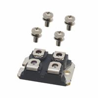
miniBLOC, SOT-227 B
M4 screws (4x) supplied
Dim.
© 2000 IXYS All rights reserved
Millimeter
Min.
Max.
Inches
Min.
Max.
A
B
31.50
7.80
31.88
8.20
1.240
0.307
1.255
0.323
C
D
4.09
4.09
4.29
4.29
0.161
0.161
0.169
0.169
E
F
4.09
14.91
4.29
15.11
0.161
0.587
0.169
0.595
G
H
30.12
38.00
30.30
38.23
1.186
1.496
1.193
1.505
J
K
11.68
8.92
12.22
9.60
0.460
0.351
0.481
0.378
L
M
0.76
12.60
0.84
12.85
0.030
0.496
0.033
0.506
N
O
25.15
1.98
25.42
2.13
0.990
0.078
1.001
0.084
P
Q
4.95
26.54
5.97
26.90
0.195
1.045
0.235
1.059
R
S
3.94
4.72
4.42
4.85
0.155
0.186
0.174
0.191
T
U
24.59
-0.05
25.07
0.1
0.968
-0.002
0.987
0.004
IXYS MOSFETS and IGBTs are covered by one or more of the following U.S. patents:
4,835,592
4,881,106
5,017,508
5,049,961
5,187,117
5,486,715
4,850,072
4,931,844
5,034,796
5,063,307
5,237,481
5,381,025
C1 - 185
�IXFN / IXFK 44N50
IXFN / IXFK 48N50
Fig. 1 Output Characteristics
100
90
6V
80
80
70
70
ID - Amperes
ID - Amperes
100
7V
VGS = 10V
TJ = 25°C
90
Fig. 2 Input Admittance
60
50
40
5V
30
TJ = 25°C
60
50
40
30
20
20
10
10
0
0
0
5
10
15
20
25
30
35
0
1
2
3
VDS - Volts
7
8
9
10
2.50
TJ = 25°C
2.25
1.4
1.3
VGS = 10V
1.2
VGS = 15V
1.1
RDS(on) - Normalized
1.5
RDS(on) - Normalized
6
Fig. 4 Temperature Dependence
of Drain to Source Resistance
1.6
1.0
2.00
1.75
ID = 24A
1.50
1.25
1.00
0.75
0.9
0
0.50
-50
10 20 30 40 50 60 70 80 90 100
-25
0
ID - Amperes
1.2
48N50
44N50
30
20
10
0
-50
75
100 125 150
VGS(th)
BVDSS
1.1
BV/VG(th) - Normalized
40
50
Fig. 6 Temperature Dependence of
Breakdown and Threshold Voltage
60
50
25
TJ - Degrees C
Fig. 5 Drain Current vs.
Case Temperature
ID - Amperes
5
VGS - Volts
Fig. 3 RDS(on) vs. Drain Current
1.0
0.9
0.8
0.7
0.6
-25
0
25
50
75
TC - Degrees C
C1 - 186
4
100 125 150
0.5
-50
-25
0
25
50
75
100 125 150
TJ - Degrees C
© 2000 IXYS All rights reserved
�IXFN / IXFK 44N50
IXFN / IXFK 48N50
Fig.7 Gate Charge Characteristic Curve
Fig.8 Capacitance Curves
10
10000
VDS = 250V
9
9000
ID = 24A
6
5
4
3
7000
5000
4000
3000
2000
1
1000
0
0
50
f = 1 MHz
VDS = 25V
6000
2
0
Ciss
8000
Capacitance - pF
VGE - Volts
8 I = 10mA
G
7
100 150 200 250 300 350 400
Coss
Crss
0
5
Gate Charge - nCoulombs
10
15
20
25
VDS - Volts
Fig.9 Source Current vs. Source
to Drain Voltage
100
90
ID - Amperes
80
70
60
50
TJ = 125°C
40
30
TJ = 25°C
20
10
0
0.00
0.25
0.50
0.75
1.00
1.25
1.50
VSD - Volt
Thermal Response - K/W
Fig.10 Transient Thermal Impedance
0.1
0.01
0.001
0.01
0.1
1
Time - Seconds
© 2000 IXYS All rights reserved
C1 - 187
�Disclaimer Notice - Information furnished is believed to be accurate and reliable. However, users should independently
evaluate the suitability of and test each product selected for their own applications. Littelfuse products are not designed for,
and may not be used in, all applications. Read complete Disclaimer Notice at www.littelfuse.com/disclaimer-electronics.
�