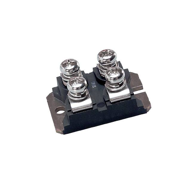
IXFN70N120SK
preliminary
SiC Power MOSFET
ID25
= 68 A
VDSS
= 1200 V
RDS(on) max = 34 mΩ
Kelvin Source gate connection
KS
Part number
IXFN70N120SK
G
D
D (3)
S
Backside: isolated
UL pending
G (2)
KS (1)
S (4)
Features / Advantages:
Applications:
Package: SOT-227B (minibloc)
• High speed switching
with low capacitances
• High blocking voltage
with low RDS(on)
• Easy to parallel and simple to drive
• Resistant to latch-up
• Real Kelvin source connection
• Solar inverters
• High voltage DC/DC converters
• Motor drives
• Switch mode power supplies
• UPS
• Battery chargers
• Induction heating
• Isolation Voltage: 3000 V~
• Industry standard outline
• RoHS compliant
• Epoxy meets UL 94V-0
• Base plate with Aluminium nitride
isolation
• Advanced power cycling
Terms & Conditions of usage
The data contained in this product data sheet is exclusively intended for technically trained staff. The user will have to evaluate the suitability of the product for the intended application and the completeness of
the product data with respect to his application. The specifications of our components may not be considered as an assurance of component characteristics. The information in the valid application- and assembly
notes must be considered. Should you require product information in excess of the data given in this product data sheet or which concerns the specific application of your product, please contact your local sales
office.
Due to technical requirements our product may contain dangerous substances. For information on the types in question please contact your local sales office.
Should you intend to use the product in aviation, in health or life endangering or life support applications, please notify. For any such application we urgently recommend
- to perform joint risk and quality assessments;
- the conclusion of quality agreements;
- to establish joint measures of an ongoing product survey, and that we may make delivery dependent on the realization of any such measures.
IXYS reserves the right to change limits, test conditions and dimensions.
© 2018 IXYS All rights reserved
20180405a
1-7
�IXFN70N120SK
preliminary
MOSFET
Ratings
Symbol
Definitions
Conditions
min.
VDSS
drain source breakdown voltage
VGS = 0 V, ID = 100 µA
1200
VGSM
VGS
max transient gate source voltage
continous gate source voltage
recommended operational value
ID25
ID80
ID100
drain current
TC = 25°C
VGS = 20 V
TC = 80°C
TC = 100°C
RDSon
static drain source on resistance
ID = 50 A; VGS = 20 V
TVJ = 25°C
TVJ = 175°C
VGS(th)
gate threshold voltage
ID = 15 mA; VGS = VDS
TVJ = 25°C
TVJ = 175°C
IDSS
drain source leakage current
VDS = 1200 V; VGS = 0 V
TVJ = 25°C
IGSS
gate source leakage current
VDS = 0 V; VGS = 20 V
TVJ = 25°C
RG
internal gate resistance
f = 1 MHz, VAC = 25 mV, ESR of CISS
Ciss
Coss
Crss
input capacitance
output capacitance
reverse transfer (Miller) capacitance
Qg
Qgs
Qgd
total gate charge
gate source charge
gate drain (Miller) charge
td(on)
tr
td(off)
tf
Eon
Eoff
Erec(off)
turn-on delay time
current rise time
turn-off delay time
current fall time
turn-on energy per pulse
turn-off energy per pulse
reverse recovery losses at turn-off
td(on)
tr
td(off)
tf
Eon
Eoff
Erec(off)
turn-on delay time
current rise time
turn-off delay time
current fall time
turn-on energy per pulse
turn-off energy per pulse
reverse recovery losses at turn-off
RthJC
RthJH
thermal resistance junction to case
thermal resistance junction to heatsink
typ.
V
-10
-5
2.0
max.
+25
+20
V
V
68
55
48
A
A
A
25
52
34
mΩ
mΩ
2.6
2.1
4.0
V
V
2
100
µA
0.6
µA
1.1
Ω
VDS = 1000 V; VGS = 0 V; f = 1 MHz TVJ = 25°C
2790
220
15
pF
pF
pF
VDS = 800 V; ID = 50 A; VGS = -5/20 V TVJ = 25°C
161
46
50
nC
nC
nC
Inductive switching
VDS = 800 V; ID = 50 A
TVJ = 25°C
VGS = -5 / 20 V; RG = 15 Ω (external)
Freewheeling diode is Mosfet's body diode
30
15
82
27
1.35
0.76
0.13
ns
ns
ns
ns
mJ
mJ
mJ
Inductive switching
VDS = 800 V; ID = 50 A
TVJ = 150°C
VGS = -5 / 20 V; RG = 15 Ω (external)
Freewheeling diode is Mosfet's body diode
28
12
125
28
1.71
0.78
0.29
ns
ns
ns
ns
mJ
mJ
mJ
0.45
with heatsink compound; IXYS test setup
0.6
Source-Drain Diode
K/W
K/W
Ratings
Symbol
Definitions
Conditions
VSD
forward voltage drop
IF = 50 A; VGS = -5 V
TVJ = 25°C
TVJ = 150°C
min.
trr
QRM
IRM
dIF/dt
reverse recovery time
reverse recovery charge (intrinsic diode)
max. reverse recovery current
current slew rate
VGS = -5 V; IF = 50 A; VR = 800 V
Mosfet gate drive:
VGS = -5 / 20 V; RG = 15 Ω
TVJ = 25°C
trr
QRM
IRM
dIF/dt
reverse recovery time
reverse recovery charge (intrinsic diode)
max. reverse recovery current
current slew rate
VGS = -5 V; IF = 50 A; VR = 800 V
Mosfet gate drive:
VGS = -5 / 20 V; RG = 15 Ω
TVJ = 150°C
typ.
max.
4.3
3.7
V
V
35
0.52
33
3380
ns
µC
A
A/µs
30
1.23
59
4250
ns
µC
A
A/µs
Note:
When using SiC Body Diode the maximum recommended VGS = -5V
IXYS reserves the right to change limits, test conditions and dimensions.
© 2018 IXYS All rights reserved
20180405a
2-7
�IXFN70N120SK
preliminary
Package SOT-227B (minibloc)
min.
Ratings
typ. max.
storage temperature
operation temperature
virtual junction temperature
-40
-40
-40
150
150
175
°C
°C
°C
MD
mounting torque
1.1
1.5
Nm
MT
terminal torque
1.1
1.5
Symbol
IRMS
Definitions
RMS current
Tstg
Top
TVJ
Conditions
per terminal
Weight
30
dSpp/App
dSpb/Apb
creepage distance on surface | striking distance through air
VISOL
isolation voltage
terminal to backside
terminal to terminal
Unit
A
g
Nm
10.5 / 3.2
8.6 / 6.8
mm
mm
3000
2500
V
V
IISOL < 1 mA; 50/60 Hz, t = 1 sec.
t = 1 minute
Product Marking
Part No.
Logo
XXXXX
yywwZ ®
abcd
DateCode
Assembly Line
Assembly Code
Ordering
Part Name
Marking on Product
Standard
IXFN70N120SK
IXFN70N120SK
IXYS reserves the right to change limits, test conditions and dimensions.
© 2018 IXYS All rights reserved
Delivering Mode Base Qty Ordering Code
Tube
10
517981
20180405a
3-7
�IXFN70N120SK
preliminary
Outlines SOT-227B (minibloc)
D (3)
G (2)
KS (1)
S (4)
IXYS reserves the right to change limits, test conditions and dimensions.
© 2018 IXYS All rights reserved
20180405a
4-7
�IXFN70N120SK
preliminary
Curves
150
150
20 V
18 V
16 V
14 V
12 V
100
12 V
20 V
18 V
16 V
14 V
100
VGS = 10 V
ID
ID
VGS = 10 V
[A]
[A]
50
50
TVJ = 25°C
TVJ = -25°C
0
0
0
1
2
3
4
5
6
7
8
9
10
0
1
2
3
4
5
VDS [V]
6
7
8
9
10
VDS [V]
Fig. 1 Typical output characteristics (-25°C)
Fig. 2 Typical output characteristics (25°C)
150
2.5
VGS = 20 V
20 V
18 V
16 V
14 V
TVJ = 150°C
100 A
2.0
12 V
100
ID = 50 A
1.5
VGS = 10 V
ID
RDS(on)
normalized
[A]
1.0
50
0.5
0
0
1
2
3
4
5
6
7
8
9
0.0
-25
10
0
25
50
VDS [V]
75
100
125
150
175
TVJ [°C]
Fig. 4 RDS(on) normalized vs. junction temperature TVJ
Fig. 3 Typical output characteristics (150°C)
80
80
VGS = 20 V
ID = 50 A
60
60
TVJ = 150°C
RDS(on)
VGS = 14 V
16 V
18 V
20 V
RDS(on)
40
40
[mOhm]
[mOhm]
25°C
-25°C
20
0
0
25
50
75
100
125
150
IDS [A]
Fig. 5 RDS(on) versus drain current
IXYS reserves the right to change limits, test conditions and dimensions.
© 2018 IXYS All rights reserved
20
0
-25
0
25
50
75
100
125
150
175
TVJ [°C]
Fig. 6 RDS(on) versus junction temperature TVJ
20180405a
5-7
�IXFN70N120SK
preliminary
Curves
1.4
3.2
150
VDS = 20 V
3.0
1.2
2.8
VDSS
IDSS =
0.1 mA
VDSS
100
2.6
VTH
1.0
2.4
normalized
2.2
[V]
TVJ = 150°C
ID
[A]
25°C
50
0.8
0.6
-25
1.8
IDSS =
15 mA
0
25
50
75
100
-55°C
2.0
VTH
125
150
1.6
175
0
0 1 2 3 4 5 6 7 8 9 10 11 12 13 14 15
TVJ [°C]
VGS [V]
Fig. 7 Norm. breakdow VDSS & treshhold voltage VTH
Fig. 8 Typical transfer characteristics
versus junction temperature TVJ
50
0
TVJ = -25°C
TVJ = -25°C
-25
40
25°C
150°C
-50
30
gfs
IDS
-5 V
-2 V
-75
[S]
[V]
20
VGS = 0 V
-100
10
-125
0
-150
0
10
20
30
40
50
60
70
80
-9
90 100
-8
-7
-6
ID [A]
-5
-4
-3
-2
-1
0
VDS [V]
Fig. 10 Forward voltage drop of intrinsic diode
versus VDS measured at -55°C
Fig. 9 Typical forward transconductance
0
0
TVJ = 150°C
TVJ = 25°C
-25
-25
-50
-50
IDS
-75
-75
-2 V
VGS = 0 V
[V]
VGS = 0 V
-100
-2 V
IDS
-5 V
[V]
-5 V
-100
-125
-125
-150
-150
-9
-8
-7
-6
-5
-4
-3
-2
-1
0
-9
-8
-7
-6
-5
-4
-3
-2
-1
0
VDS [V]
VDS [V]
Fig. 11 Forward voltage drop of intrinsic diode
versus VDS measured at 25°C
Fig. 12 Forward voltage drop of intrinsic diode
versus VDS measured at 150°C
IXYS reserves the right to change limits, test conditions and dimensions.
© 2018 IXYS All rights reserved
20180405a
6-7
�IXFN70N120SK
preliminary
Curves
3.0
5
RG = 15 Ω
TVJ = 150°C
VDS = 800 V
VGS = -5/20 V
4
RG = 15 Ω
VDS = 800 V
VGS = -5/20 V
ID = 50 A
2.5
2.0
3
Erec x10
E
E
Eon
1.5
Erec x10
[mJ] 2
[mJ]
1.0
1
Eon
0.5
Eoff
0
0
10
Eoff
20
30
40
50
60
70
80
0.0
20
90 100
40
60
80
ID [A]
Fig. 13 Typical switching energy
versus drain current
ID = 50 A
TVJ = 150°C
VDS = 800 V
VGS = -5/20 V
2.5
120
140
Eon
ID = 50 A
TVJ = 150°C
VDS = 800 V
VGS = -5/20 V
200
160
2.0
E
t
Eoff
1.5
120
td(off)
[ns]
[mJ]
1.0
80
0.5
40
td(on)
Erec
0.0
6
12
18
24
30
6
36
12
18
30
36
Fig. 16 Typical switching time versus
external gate resistor
0.7
ID = 40 A
TVJ = 25°C
15 VDS = 800 V
IGS = 10 mA
[V]
24
RG [Ω]
Fig. 15 Typical switching energy versus
external gate resistor
20
tf
tr
0
RG [Ω]
VGS
160
Fig. 14 Typical switching energy
versus temperature
240
3.0
100
TVJ [°C]
0.6
0.5
10
Zth(J-H) 0.4
[K/W] 0.3
5
0.2
0
0.1
-5
0
20
40
60
80
100 120 140 160 180
QG [nC]
Fig. 17 Typical turn on gate charge, trendline
IXYS reserves the right to change limits, test conditions and dimensions.
© 2018 IXYS All rights reserved
0.0
1
10
100
1000
10000
tp [ms]
Fig. 18 Typical transient thermal impedance
20180405a
7-7
�
很抱歉,暂时无法提供与“IXFN70N120SK”相匹配的价格&库存,您可以联系我们找货
免费人工找货