PolarHVTM HiPerFET
Power MOSFET
IXFN 80N50P
VDSS
ID25
RDS(on)
trr
N-Channel Enhancement Mode
Avalanche Rated
Fast Intrinsic Diode
Symbol
Test Conditions
VDSS
VDGR
TJ = 25° C to 150° C
TJ = 25° C to 150° C; RGS = 1 MΩ
500
500
V
V
VGS
VGSM
Transient
Continuous
± 40
± 30
V
V
ID25
IDM
TC = 25° C
TC = 25° C, pulse width limited by TJM
66
200
A
A
IAR
EAR
EAS
TC = 25° C
TC = 25° C
TC = 25° C
80
80
3.0
A
mJ
J
dv/dt
IS ≤ IDM, di/dt ≤ 100 A/µs, VDD ≤ VDSS,
TJ ≤150° C, RG = 2 Ω
10
V/ns
PD
TC = 25° C
700
W
Maximum Ratings
-55 ... +150
150
-55 ... +150
°C
°C
°C
300
°C
2500
V~
TJ
TJM
Tstg
TL
1.6 mm (0.062 in.) from case for 10 s
VISOL
50/60 Hz; IISOL ≤1
Md
Mounting torque
Terminal connection torque (M4)
mA
1.5/13 Nm/ib.in.
1.5/13 Nm/ib.in.
Weight
30
Symbol
Test Conditions
(TJ = 25° C unless otherwise specified)
g
Characteristic Values
Min. Typ.
Max.
BVDSS
VGS = 0 V, ID = 500 µA
500
VGS(th)
VDS = VGS, ID = 8 mA
3.0
IGSS
VGS = ± 30 VDC, VDS = 0
IDSS
VDS = VDSS
VGS = 0 V
RDS(on)
VGS = 10 V, ID = 0.5 ID25, Note 1
© 2006 IXYS All rights reserved
= 500 V
= 66 A
Ω
≤
65 mΩ
≤ 200 ns
TJ = 125° C
V
5.0
V
± 200
nA
25
1
µA
mA
65
mΩ
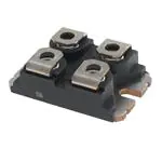
miniBLOC, SOT-227 B (IXFN)
E153432
S
G
S
D
G = Gate
S = Source
D = Drain
Either source tab S can be used forsource
current or Kelvin gate return.
Features
l
Fast intrinsic diode
l
International standard package
l
Unclamped Inductive Switching (UIS)
rated
l
UL recognized.
l
Isolated mounting base
Advantages
l
Easy to mount
l
Space savings
l
High power density
DS99477E(01/06)
�IXFN 80N50P
Symbol
Test Conditions
Characteristic Values
(TJ = 25° C unless otherwise specified)
Min.
Typ.
Max.
gfs
VDS= 20 V; ID = 0.5 ID25, Note 1
35
Ciss
70
S
12.7
nF
1280
pF
Crss
120
pF
td(on)
25
ns
Coss
VGS = 0 V, VDS = 25 V, f = 1 MHz
tr
VGS = 10 V, VDS = 0.5 VDSS, ID = 0.5*ID25
27
ns
td(off)
RG = 2 Ω (External)
70
ns
18
ns
195
nC
70
nC
64
nC
tf
Qg(on)
Qgs
VGS= 10 V, VDS = 0.5 VDSS, ID = 0.5 ID25
Qgd
RthJC
miniBLOC, SOT-227B (IXFN) Outline
0.18° C/W
RthCK
° C/W
0.05
Source-Drain Diode
Characteristic Values
TJ = 25° C unless otherwise specified)
Min.
Typ.
Max.
Symbol
Test Conditions
IS
VGS = 0 V
80
A
ISM
Repetitive
200
A
VSD
IF = IS, VGS = 0 V, Note 1
1.5
V
trr
IF = 25 A, -di/dt = 100 A/µs
200
ns
QRM
VR = 100 V, VGS = 0 V
0.8
µC
8
A
IRM
Note 1: Pulse test, t ≤300 µs, duty cycle d ≤ 2 %
IXYS reserves the right to change limits, test conditions, and dimensions.
IXYS MOSFETs and IGBTs are covered by 4,835,592
one or more of the following U.S. patents: 4,850,072
4,881,106
4,931,844
5,017,508
5,034,796
5,049,961
5,063,307
5,187,117
5,237,481
5,381,025
5,486,715
6,162,665
6,259,123 B1
6,306,728 B1
6,404,065 B1
6,534,343
6,583,505
6,683,344
6,710,405B2
6,710,463
6,727,585
6,759,692
6771478 B2
�IXFN 80N50P
Fig. 1. Output Characte r is tics
Fig. 2. Exte nde d Output Char acte ris tics
@ 25° C
V GS = 10V
70
V GS = 10V
160
8V
60
8V
140
7V
120
50
I D - Amperes
I D - Amperes
@ 25° C
180
80
40
30
6V
20
7V
100
80
60
6V
40
10
20
5V
5V
0
0
0
1
2
3
4
5
6
0
3
6
9
V D S - V olts
Fig. 3. Output Characte r is tics
80
18
21
24
27
3.4
V GS = 10V
70
3.1
R D S ( o n ) - Normalized
7V
60
I D - Amperes
15
Fig. 4. RDS(on ) Norm alize d to ID = 40A
V alue vs . Junction Te m pe rature
@ 125° C
6V
50
40
30
20
5V
10
V GS = 10V
2.8
2.5
2.2
I D = 80A
1.9
1.6
I D = 40A
1.3
1
0.7
0
0.4
0
2
4
6
8
10
12
14
-50
-25
V D S - V olts
0
25
50
75
100
125
150
TJ - Degrees Centigrade
Fig. 5. RDS(on) Norm alize d to ID = 40A
V alue vs . Drain Curr e nt
Fig. 6. Dr ain Cur r e nt vs . Cas e
T e m p e r atur e
3.2
70
3
V GS = 10V
60
TJ = 125 ° C
2.8
2.6
50
2.4
I D - Amperes
R D S ( o n ) - Normalized
12
V D S - V olts
2.2
2
1.8
1.6
1.4
1.2
TJ = 25 ° C
1
40
30
20
10
0.8
0
0
20
40
60
80
100
120
I D - A mperes
© 2006 IXYS All rights reserved
140
160
180
-50
-25
0
25
50
75
100
TC - Degrees Centigrade
125
150
�IXFN 80N50P
Fig. 8. Transconductance
140
140
120
120
100
100
80
g f s - Siemens
I D - Amperes
Fig. 7. Input Adm ittance
TJ = 125°C
25°C
60
-40°C
TJ = -40°C
25°C
125°C
80
60
40
40
20
20
0
0
4
4.5
5
5.5
6
6.5
7
0
7.5
20
40
V G S - Volts
Fig. 9. Source Current vs.
Source-To-Drain Voltage
80
100
120
140
Fig. 10. Gate Charge
10
250
VDS = 250V
9
VG S - Volts
200
I S - Amperes
60
I D - Amperes
150
100
8
I D = 40A
7
I G = 10mA
6
5
4
3
TJ = 125°C
50
2
TJ = 25°C
1
0
0
0.4
0.6
0.8
1
1.2
1.4
1.6
0
20
40
60
V S D - Volts
80
100 120 140 160 180 200
Q G - NanoCoulombs
Fig. 12. Forw ard-Bias
Safe Operating Area
Fig. 11. Capacitance
100000
1000
R DS(on) Limit
10000
C iss
I D - Amperes
Capacitance - PicoFarads
f = 1MHz
1000
C oss
100
25µs
100µs
1ms
10
100
TJ = 150°C
C rss
DC
10ms
TC = 25°C
10
1
0
5
10
15
20
25
30
35
40
V D S - Volts
IXYS reserves the right to change limits, test conditions, and dimensions.
10
100
V D S - Volts
1000
�IXFN 80N50P
Fig. 13. Maxim um Transient Therm al Resistance
R ( t h ) J C - ºC / W
1.00
0.10
0.01
0.0001
0.001
0.01
0.1
Pulse Width - Seconds
© 2006 IXYS All rights reserved
1
10
�Disclaimer Notice - Information furnished is believed to be accurate and reliable. However, users should independently
evaluate the suitability of and test each product selected for their own applications. Littelfuse products are not designed for,
and may not be used in, all applications.Read complete Disclaimer Notice at www.littelfuse.com/disclaimer-electronics.
�


 工商网监
湘ICP备2023018690号
工商网监
湘ICP备2023018690号

