Advance Technical Information
VDSS
ID25
IXFP5N100PM
PolarTM HiPerFETTM
Power MOSFET
RDS(on)
(Electrically Isolated Tab)
N-Channel Enhancement Mode
Avalanche Rated
= 1000V
= 2.3A
Ω
≤ 2.8Ω
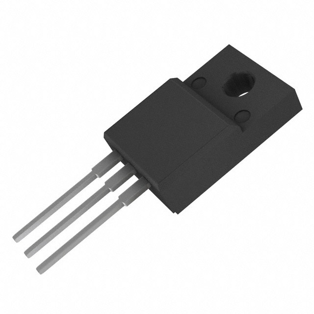
OVERMOLDED
(IXFP...M) OUTLINE
Symbol
Test Conditions
Maximum Ratings
VDSS
TJ = 25°C to 150°C
1000
V
VDGR
TJ = 25°C to 150°C, RGS = 1MΩ
1000
V
VGSS
Continuous
±30
V
VGSM
Transient
±40
V
ID25
TC = 25°C
2.3
A
IDM
TC = 25°C, Pulse Width Limited by TJM
10
A
G
G = Gate
S = Source
IA
TC = 25°C
5
A
EAS
TC = 25°C
300
mJ
dv/dt
IS ≤ IDM, VDD ≤ VDSS, TJ ≤ 150°C
10
V/ns
PD
TC = 25°C
42
W
-55 ... +150
°C
TJM
150
°C
z
Tstg
-55 ... +150
°C
z
300
260
°C
°C
1.13 / 10
Nm/lb.in.
2.5
g
TJ
TL
TSOLD
Maximum Lead Temperature for Soldering
Plastic Body for 10s
Md
Mounting Torque
Weight
DS
Isolated Tab
D = Drain
Features
z
z
z
Plastic overmolded Tab for Electrical
Isolation
Low RDS(on) and QG
Avalanche Rated
Low Package Inductance
Fast Intrinsic Rectifier
Advantages
z
z
z
High Power Density
Easy to Mount
Space Savings
Applications
Symbol
Test Conditions
(TJ = 25°C Unless Otherwise Specified)
BVDSS
VGS = 0V, ID = 250μA
1000
VGS(th)
VDS = VGS, ID = 250μA
3.0
IGSS
VGS = ± 30V, VDS = 0V
IDSS
VDS = VDSS, VGS = 0V
z
V
6.0
V
±100 nA
z
z
z
Switch-Mode and Resonant-Mode
Power Supplies
DC-DC Converters
Laser Drivers
AC and DC Motor Drives
Robotics and Servo Controls
10 μA
TJ = 125°C
RDS(on)
z
Characteristic Values
Min. Typ.
Max.
VGS = 10V, ID = 2.5A, Note 1
© 2013 IXYS CORPORATION, All Rights Reserved.
750 μA
2.8
Ω
DS100537(5/13)
�IXFP5N100PM
Symbol
Test Conditions
(TJ = 25°C Unless Otherwise Specified)
Characteristic Values
Min.
Typ.
Max.
gfs
2.4
VDS = 20V, ID = 2.5A, Note 1
Ciss
Coss
4.0
S
1830
pF
113
pF
20
pF
1.6
Ω
12
ns
13
ns
30
ns
37
ns
33.4
nC
10.6
nC
14.4
nC
VGS = 0V, VDS = 25V, f = 1MHz
Crss
RGi
Gate Input Resistance
td(on)
Resistive Switching Times
tr
td(off)
tf
VGS = 10V, VDS = 0.5 • VDSS, ID = 2.5A
RG = 5Ω (External)
Qg(on)
Qgs
OVERMOLDED TO-220 FULL PAK
VGS = 10V, VDS = 0.5 • VDSS, ID = 2.5A
Qgd
3.0 °C/W
RthJC
1
2
Terminals:
3
1 - Gate
2 - Drain
3 - Source
Source-Drain Diode
Symbol
Test Conditions
(TJ = 25°C Unless Otherwise Specified)
IS
VGS = 0V
ISM
VSD
trr
IRM
QRM
Note:
Characteristic Values
Min.
Typ.
Max.
5
A
Repetitive, Pulse Width Limited by TJM
20
A
IF = IS, VGS = 0V, Note 1
1.3
V
200
ns
IF = 5A, -di/dt = 100A/μs
VR = 100V, VGS = 0V
7.4
A
0.43
μC
1. Pulse test, t ≤ 300μs, duty cycle, d ≤ 2%.
ADVANCE TECHNICAL INFORMATION
The product presented herein is under development. The Technical Specifications offered are
derived from a subjective evaluation of the design, based upon prior knowledge and experience, and constitute a "considered reflection" of the anticipated result. IXYS reserves the right
to change limits, test conditions, and dimensions without notice.
IXYS Reserves the Right to Change Limits,Test Conditions, and Dimensions.
IXYS MOSFETs and IGBTs are covered
4,835,592
by one or moreof the following U.S. patents: 4,860,072
4,881,106
4,931,844
5,017,508
5,034,796
5,049,961
5,063,307
5,187,117
5,237,481
5,381,025
5,486,715
6,162,665
6,259,123 B1
6,306,728 B1
6,404,065 B1
6,534,343
6,583,505
6,683,344
6,727,585
7,005,734 B2
6,710,405 B2 6,759,692
7,063,975 B2
6,710,463
6,771,478 B2 7,071,537
7,157,338B2
�IXFP5N100PM
Fig. 2. Extended Output Characteristics @ T J = 25ºC
Fig. 1. Output Characteristics @ T J = 25ºC
5.0
8
VGS = 10V
8V
4.5
VGS = 10V
9V
8V
7
4.0
6
7V
ID - Amperes
ID - Amperes
3.5
3.0
2.5
2.0
5
7V
4
3
1.5
2
6V
1.0
5V
0.0
0
0
2
4
6
8
10
12
14
0
5
10
15
20
25
30
VDS - Volts
VDS - Volts
Fig. 3. Output Characteristics @ T J = 125ºC
Fig. 4. RDS(on) Normalized to ID = 2.5A Value vs.
Junction Temperature
5.0
2.8
VGS = 10V
8V
4.5
VGS = 10V
2.4
3.5
R DS(on) - Normalized
4.0
ID - Amperes
6V
1
0.5
7V
3.0
2.5
2.0
6V
1.5
1.0
I D = 5A
2.0
I D = 2.5A
1.6
1.2
0.8
5V
0.5
0.0
0.4
0
3
6
9
12
15
18
21
24
27
30
-50
-25
0
25
VDS - Volts
50
75
100
125
150
125
150
TJ - Degrees Centigrade
Fig. 5. RDS(on) Normalized to ID = 2.5A Value vs.
Drain Current
Fig. 6. Maximum Drain Current vs.
Case Temperature
2.6
2.5
VGS = 10V
2.4
TJ = 125ºC
2.0
2.0
ID - Amperes
R DS(on) - Normalized
2.2
1.8
1.6
1.5
1.0
1.4
1.2
0.5
TJ = 25ºC
1.0
0.8
0.0
0
1
2
3
4
5
ID - Amperes
© 2013 IXYS CORPORATION, All Rights Reserved.
6
7
8
-50
-25
0
25
50
75
TC - Degrees Centigrade
100
�IXFP5N100PM
Fig. 7. Input Admittance
Fig. 8. Transconductance
6
4.5
TJ = - 40ºC
4
25ºC
4
g f s - Siemens
ID - Amperes
5
TJ = 125ºC
25ºC
- 40ºC
3.5
3
2.5
2
125ºC
3
1.5
2
1
1
0.5
0
0
4.0
4.5
5.0
5.5
6.0
6.5
7.0
7.5
0
0.5
1
1.5
VGS - Volts
2
2.5
3
3.5
4
4.5
ID - Amperes
Fig. 10. Gate Charge
Fig. 9. Forward Voltage Drop of Intrinsic Diode
10
16
VDS = 500V
9
14
I D = 2.5A
8
I G = 10mA
12
10
VGS - Volts
IS - Amperes
7
8
6
6
5
4
TJ = 125ºC
3
TJ = 25ºC
4
2
2
1
0
0
0.4
0.5
0.6
0.7
0.8
0.9
1.0
1.1
0
1.2
4
8
VSD - Volts
12
16
20
24
28
32
QG - NanoCoulombs
Fig. 12. Maximum Transient Thermal Impedance
Fig. 11. Capacitance
10,000
10
f = 1 MHz
1,000
Z(th)JC - ºC / W
Capacitance - PicoFarads
Ciss
Coss
100
1
0.1
Crss
10
0
5
10
15
20
25
30
35
40
VDS - Volts
0.01
0.0001
0.001
0.01
0.1
1
10
100
Pulse Width - Seconds
IXYS Reserves the Right to Change Limits,Test Conditions, and Dimensions.
IXYS REF: F_5N100P(55-744)5-07-13-A
�Disclaimer Notice - Information furnished is believed to be accurate and reliable. However, users should independently
evaluate the suitability of and test each product selected for their own applications. Littelfuse products are not designed for,
and may not be used in, all applications. Read complete Disclaimer Notice at www.littelfuse.com/disclaimer-electronics.
�