PolarHVTM HiPerFET
Power MOSFET
N-Channel Enhancement Mode
Avalanche Rated
Fast Intrinsic Diode
VDSS
ID25
IXFH 30N50P
IXFT 30N50P
IXFV 30N50P
IXFV 30N50PS
RDS(on)
trr
= 500 V
= 30 A
≤ 200 mΩ
Ω
≤ 200 ns
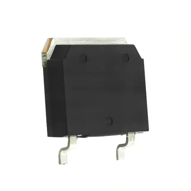
TO-247 AD (IXFH)
Symbol
Test Conditions
Maximum Ratings
VDSS
TJ = 25° C to 150° C
500
V
VDGR
TJ = 25° C to 150° C; RGS = 1 MΩ
500
V
VGSS
Continuous
±30
V
VGSM
Transient
±40
V
ID25
IDM
TC = 25° C
TC = 25° C, pulse width limited by TJM
30
75
A
A
IAR
EAR
EAS
TC = 25° C
TC = 25° C
TC = 25° C
30
40
1.2
A
mJ
J
dv/dt
IS ≤ IDM, di/dt ≤ 100 A/µs, VDD ≤ VDSS,
TJ ≤150° C, RG = 5 Ω
10
V/ns
PD
TC = 25° C
460
W
-55 ... +150
150
-55 ... +150
°C
°C
°C
300
260
°C
°C
TJ
TJM
Tstg
TL
TSOLD
1.6 mm (0.062 in.) from case for 10 s
Plastic body for 10 s
Md
FC
Mounting torque (TO-247, TO-3P)
Mounting force (PLUS220, PLUS220SMD)
Weight
PLUS220, PLUS220SMD
TO-268
TO-247
Symbol
1.13/10 Nm/lb.in
11 65/2.5 15 N/lb.
4
5
6
Test Conditions
(TJ = 25° C, unless otherwise specified)
g
g
g
Characteristic Values
Min. Typ. Max.
BVDSS
VGS = 0 V, ID = 250 µA
500
VGS(th)
VDS = VGS, ID = 4 mA
3.0
IGSS
VGS = ±30 V, VDS = 0 V
±100
nA
IDSS
VDS = VDSS
VGS = 0 V
25
750
µA
µA
RDS(on)
VGS = 10 V, ID = 0.5 ID25
Pulse test, t ≤300 µs, duty cycle d ≤ 2 %
200
mΩ
© 2006 IXYS All rights reserved
V
5.0
TJ = 125° C
165
V
D (TAB)
TO-268 (IXFT)
G
S
D (TAB)
PLUS220 (IXFV)
G
D
S
D (TAB)
PLUS220 SMD(IXFV..S)
G
S
G = Gate
S = Source
D (TAB)
D = Drain
TAB = Drain
Features
l
International standard packages
l
Unclamped Inductive Switching (UIS)
rated
l
Low package inductance
- easy to drive and to protect
Advantages
l
Easy to mount
l
Space savings
l
High power density
DS99414E(04/06)
�IXFH 30N50P IXFT 30N50P
IXFV 30N50P IXFV 30N50PS
Symbol
Test Conditions
Characteristic Values
(TJ = 25° C, unless otherwise specified)
Min.
Typ.
Max.
gfs
VDS= 20 V; ID = 0.5 ID25, pulse test
17
Ciss
Coss
VGS = 0 V, VDS = 25 V, f = 1 MHz
27
S
4150
pF
445
pF
Crss
28
pF
td(on)
25
ns
tr
VGS = 10 V, VDS = 0.5 VDSS, ID = 0.5 ID25
24
ns
td(off)
RG = 5 Ω (External)
82
ns
tf
24
ns
Qg(on)
70
nC
27
nC
22
nC
VGS= 10 V, VDS = 0.5 VDSS, ID = 0.5 ID25
Qgs
Qgd
0.27° C/W
RthJC
RthCs
(TO-247, PLUS220)
° C/W
0.21
Source-Drain Diode
Characteristic Values
(TJ = 25° C, unless otherwise specified)
Min.
Typ.
Max.
Symbol
Test Conditions
IS
VGS = 0 V
30
A
ISM
Repetitive
90
A
VSD
IF = IS, VGS = 0 V,
Pulse test, t ≤ 300 µs, duty cycle d ≤ 2 %
1.5
V
trr
IF = 25 A; -di/dt = 100 A/µs
200 ns
IRM
VR = 100 V; VGS = 0 V
QRM
6
A
0.6
µC
Characteristic Curves
Fig. 1. Output Characteristics
Fig. 2. Extended Output Characteristics
@ 25ºC
@ 25ºC
30
70
VGS = 10V
VGS = 10V
27
8V
24
50
7V
I D - Amperes
21
I D - Amperes
8V
60
18
15
12
9
6V
7V
40
30
20
6
10
3
0
6V
0
0
1
2
3
4
5
6
7
0
3
6
9
V D S - Volts
12
15
18
21
24
V D S - Volts
IXYS reserves the right to change limits, test conditions, and dimensions.
IXYS MOSFETs and IGBTs are covered by 4,835,592
one or moreof the following U.S. patents: 4,850,072
4,881,106
4,931,844
5,017,508
5,034,796
5,049,961
5,063,307
5,187,117
5,237,481
5,381,025
5,486,715
6,162,665
6,259,123 B1
6,306,728 B1
6,404,065 B1
6,534,343
6,583,505
6,683,344
6,710,405B2
6,710,463
6,727,585
6,759,692
6,771,478 B2
27
30
�IXFH 30N50P IXFT 30N50P
IXFV 30N50P IXFV 30N50PS
Fig. 3. Output Characteristics
Fig. 4. RDS(on) Norm alized to 0.5 ID25
Value vs. Junction Tem perature
@ 125ºC
30
3.4
VGS = 10V
27
R D S ( o n ) - Normalized
I D - Amperes
24
VGS = 10V
3.1
8V
7V
21
18
6V
15
12
9
6
5V
3
2.8
2.5
2.2
I D = 30A
1.9
1.6
I D = 15A
1.3
1
0.7
0
0.4
0
2
4
6
8
10
12
14
-50
-25
0
V D S - Volts
Fig. 5. RDS(on) Norm alized to
3.4
75
100
125
150
35
VGS = 10V
3.1
TJ = 125º C
30
2.8
25
2.5
I D - Amperes
R D S ( o n ) - Normalized
50
Fig. 6. Drain Current vs. Case
Tem perature
0.5 ID25 Value vs. ID
2.2
1.9
1.6
20
15
10
1.3
TJ = 25º C
5
1
0.7
0
0
10
20
30
40
50
60
70
80
-50
-25
I D - Amperes
55
45
50
40
45
g f s - Siemens
60
50
35
30
TJ = 125º C
20
25º C
15
25
50
75
100
125
150
Fig. 8. Transconductance
55
25
0
TC - Degrees Centigrade
Fig. 7. Input Adm ittance
I D - Amperes
25
TJ - Degrees Centigrade
-40º C
TJ = -40º C
40
25º C
35
125º C
30
25
20
15
10
10
5
5
0
0
3.5
4
4.5
5
5.5
V G S - Volts
© 2006 IXYS All rights reserved
6
6.5
7
7.5
0
5
10
15
20
25
30
35
I D - Amperes
40
45
50
55
�IXFH 30N50P IXFT 30N50P
IXFV 30N50P IXFV 30N50PS
Fig. 10. Gate Charge
90
10
80
9
VDS = 250V
70
8
I D = 15A
7
I G = 10mA
60
VG S - Volts
I S - Amperes
Fig. 9. Source Current vs.
Source-To-Drain Voltage
50
40
TJ = 125º C
30
5
4
3
TJ = 25º C
20
6
2
10
1
0
0
0.4
0.5
0.6
0.7
0.8
0.9
1
1.1
0
10
20
V S D - Volts
30
40
50
60
70
Q G - nanoCoulombs
Fig. 12. Forw ard-Bias
Safe Operating Area
Fig. 11. Capacitance
10000
100
C iss
1000
I D - Amperes
Capacitance - picoFarads
R DS(on) Limit
C oss
25µs
100µs
10
1ms
100
C rs
10ms
DC
TJ = 150ºC
TC = 25ºC
f = 1MHz
10
1
0
5
10
15
20
25
30
35
40
10
100
V D S - Volts
1000
V D S - Volts
Fig. 13. M axim um Tr ans ie nt The r m al Re s is tance
R ( t h ) J C - ºC / W
1.00
0.10
0.01
0.1
1
10
Pulse Width - milliseconds
IXYS reserves the right to change limits, test conditions, and dimensions.
100
1000
�IXFH 30N50P IXFT 30N50P
IXFV 30N50P IXFV 30N50PS
Package Outline Drawings
TO-247 (IXFH) Outline
1
2
3
Terminals: 1 - Gate
3 - Source
Dim.
TO-268 (IXFT) Outline
Millimeter
Min. Max.
A
4.7
5.3
2.2
2.54
A1
A2
2.2
2.6
b
1.0
1.4
1.65
2.13
b1
b2
2.87
3.12
C
.4
.8
D
20.80 21.46
E
15.75 16.26
e
5.20
5.72
L
19.81 20.32
L1
4.50
∅P 3.55
3.65
Q
5.89
6.40
R
4.32
5.49
S
6.15 BSC
2 - Drain
Tab - Drain
Inches
Min. Max.
.185 .209
.087 .102
.059 .098
.040 .055
.065 .084
.113 .123
.016 .031
.819 .845
.610 .640
0.205 0.225
.780 .800
.177
.140 .144
0.232 0.252
.170 .216
242 BSC
PLUS220SMD (IXFV_S) Outline
© 2006 IXYS All rights reserved
PLUS220 (IXFV) Outline
�Disclaimer Notice - Information furnished is believed to be accurate and reliable. However, users should independently
evaluate the suitability of and test each product selected for their own applications. Littelfuse products are not designed for,
and may not be used in, all applications.Read complete Disclaimer Notice at www.littelfuse.com/disclaimer-electronics.
�


 工商网监
湘ICP备2023018690号
工商网监
湘ICP备2023018690号
