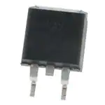
IGBT
IXGA 20N100 VCES
IXGP 20N100 IC25
VCE(sat)
= 1000 V
=
40 A
=
3.0 V
Preliminary Data Sheet
Symbol
Test Conditions
Maximum Ratings
VCES
TJ = 25°C to 150°C
1000
V
VCGR
TJ = 25°C to 150°C; RGE = 1 MΩ
1000
V
VGES
Continuous
±20
V
VGEM
Transient
±30
V
IC25
TC = 25°C
40
A
IC90
TC = 90°C
20
A
ICM
TC = 25°C, 1 ms
80
A
ICM = 40
A
SSOA
VGE = 15 V, TVJ = 125°C, RG = 47 Ω
(RBSOA)
Clamped inductive load, L = 300 µH
PC
TC = 25°C
W
-55 ... +150
°C
150
°C
Tstg
-55 ... +150
°C
300
°C
Maximum lead temperature for soldering
1.6 mm (0.062 in.) from case for 10 s
Weight
TO-220
TO-263
0.45/4 Nm/lb.in.
0.55/5 Nm/lb.in.
4
2
g
g
CE
TO-263 AA (IXGA)
G
150
TJM
Mounting torque with screw M3
Mounting torque with screw M3.5
G
@ 0.8 VCES
TJ
Md
TO-220AB (IXGP)
C (TAB)
E
Features
• International
standard packages
JEDEC TO-220AB and TO-263AA
High current handling capability
•
• MOS Gate turn-on
- drive simplicity
Applications
Symbol
Test Conditions
(TJ = 25°C, unless otherwise specified)
Min.
BVCES
IC = 1 mA, VGE = 0 V
1000
VGE(th)
IC = 250 µA, VCE = VGE
ICES
VCE = VCES
VGE = 0 V
IGES
VCE = 0 V, VGE = ±20 V
VCE(sat)
IC = ICE90, VGE = 15
© 2003 IXYS All rights reserved
Characteristic Values
Typ.
Max.
V
2.5
5.0
V
TJ = 25°C
250
µA
TJ = 125°C
1
mA
±100
nA
3.0
V
2.2
•
•
•
•
•
AC motor speed control
DC servo and robot drives
•
Capacitor discharge
DC choppers
Uninterruptible power supplies (UPS)
Switch-mode and resonant-mode
power supplies
Advantages
•
•
•
Easy to mount with one screw
Reduces assembly time and cost
High power density
DS98615B(01/03)
�IXGA 20N100
IXGP 20N100
Symbol
Test Conditions
(TJ = 25°C, unless otherwise specified)
gfs
TO-220 AB Dimensions
Characteristic Values
Min. Typ. Max.
IC = IC90; VCE = 10 V,
12
16
S
Pulse test, t ≤ 300 µs, duty cycle ≤ 2 %
Cies
Coes
VCE = 25 V, VGE = 0 V, f = 1 MHz
1750
pF
100
pF
38
pF
90
A
73
nC
13
nC
26
nC
30
ns
Cres
IC(ON)
VGE = 10V, VCE = 10V
Qg
Qge
IC = IC90, VGE = 15 V, VCE = 0.5 VCES
Qgc
td(on)
Inductive load, TJ = 25°°C
tri
IC
td(off)
tfi
Eoff
td(on)
tri
Eon
td(off)
tfi
Eoff
= IC90, VGE = 15 V
30
VCE = 800 V, RG = Roff = 47 Ω
Remarks: Switching times may
increase for VCE (Clamp) > 0.8 VCES,
higher TJ or increased RG
IC
= IC90, VGE = 15 V
VCE = 800 V, RG = Roff = 47 Ω
Remarks: Switching times may
increase for VCE (Clamp) > 0.8 VCES,
higher TJ or increased RG
700
ns
280
700
ns
3.5
8.0
mJ
30
ns
30
ns
0.65
mJ
700
ns
520
ns
6.5
mJ
RthJC
RthCK
0.83
TO-220
2 - Collector
4 - Collector
Bottom Side
ns
350
Inductive load, TJ = 125°°C
Pins: 1 - Gate
3 - Emitter
0.5
K/W
TO-263 AA Outline
K/W
1.
2.
3.
4.
Min. Recommended Footprint
(Dimensions in inches and mm)
Gate
Collector
Emitter
Collector
Bottom Side
Dim.
Millimeter
Min.
Max.
Inches
Min.
Max.
A
A1
4.06
2.03
4.83
2.79
.160
.080
.190
.110
b
b2
0.51
1.14
0.99
1.40
.020
.045
.039
.055
c
c2
0.46
1.14
0.74
1.40
.018
.045
.029
.055
D
D1
8.64
7.11
9.65
8.13
.340
.280
.380
.320
E
E1
e
9.65
6.86
2.54
10.29
8.13
BSC
.380
.270
.100
.405
.320
BSC
L
L1
L2
L3
L4
14.61
2.29
1.02
1.27
0
15.88
2.79
1.40
1.78
0.38
.575
.090
.040
.050
0
.625
.110
.055
.070
.015
R
0.46
0.74
.018
.029
IXYS reserves the right to change limits, test conditions, and dimensions.
IXYS MOSFETs and IGBTs are covered by one or more of the following U.S. patents:
4,835,592
4,850,072
4,881,106
4,931,844
5,017,508
5,034,796
5,049,961
5,063,307
5,187,117
5,237,481
5,486,715
5,381,025
6,306,728B1
�Disclaimer Notice - Information furnished is believed to be accurate and reliable. However, users should independently
evaluate the suitability of and test each product selected for their own applications. Littelfuse products are not designed for,
and may not be used in, all applications. Read complete Disclaimer Notice at www.littelfuse.com/disclaimer-electronics.
�
