Low VCE(sat) IGBT with Diode
High speed IGBT with Diode
IXGH 17 N100U1
IXGH 17 N100AU1
VCES
IC25
VCE(sat)
1000 V
1000 V
34 A
34 A
3.5 V
4.0 V
Combi Packs
Symbol
Test Conditions
Maximum Ratings
VCES
TJ = 25°C to 150°C
1000
V
VCGR
TJ = 25°C to 150°C; RGE = 1 MΩ
1000
V
VGES
Continuous
±20
V
VGEM
Transient
±30
V
IC25
TC = 25°C
34
A
IC90
TC = 90°C
17
A
ICM
TC = 25°C, 1 ms
68
A
SSOA
(RBSOA)
VGE = 15 V, TVJ = 125°C, RG = 82 Ω
Clamped inductive load, L = 100 µH
ICM = 34
@ 0.8 VCES
A
PC
TC = 25°C
150
W
-55 ... +150
°C
TJM
150
°C
Tstg
-55 ... +150
°C
TJ
Md
Mounting torque (M3)
6
Maximum lead temperature for soldering
1.6 mm (0.062 in.) from case for 10 s
G
C
E
G = Gate,
E = Emitter,
C = Collector,
TAB = Collector
Features
1.13/10 Nm/lb.in.
Weight
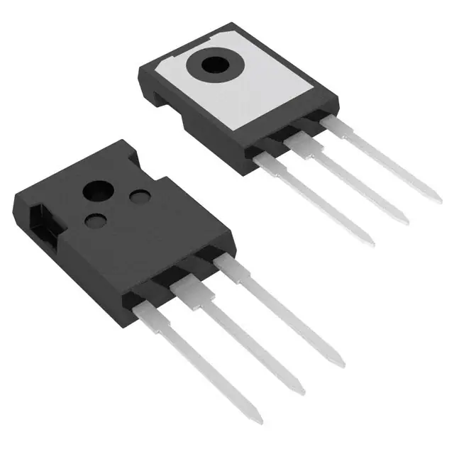
TO-247 AD
l
l
l
l
g
°C
300
l
l
International standard package
JEDEC TO-247 AD
IGBT and anti-parallel FRED in one
package
2nd generation HDMOSTM process
Low VCE(sat)
- for minimum on-state conduction
losses
MOS Gate turn-on
- drive simplicity
Fast Recovery Epitaxial Diode (FRED)
- soft recovery with low IRM
Applications
Symbol
Test Conditions
Characteristic Values
(TJ = 25°C, unless otherwise specified)
min. typ. max.
l
l
l
l
BVCES
IC
= 4.5 mA, VGE = 0 V
1000
VGE(th)
IC
= 500 µA, VCE = VGE
2.5
ICES
VCE = 0.8 • VCES
VGE = 0 V
IGES
VCE = 0 V, VGE = ±20 V
VCE(sat)
IC
= IC90, VGE = 15 V
TJ = 25°C
TJ = 125°C
17N100U1
17N100AU1
V
5.5
V
500
8
µA
mA
±100
nA
3.5
4.0
V
V
l
Advantages
l
l
l
© 1996 IXYS All rights reserved
AC motor speed control
DC servo and robot drives
DC choppers
Uninterruptible power supplies (UPS)
Switch-mode and resonant-mode
power supplies
Saves space (two devices in one
package)
Easy to mount (isolated mounting
screw hole)
Reduces assembly time and cost
91754D (3/96)
�IXGH 17N100U1
IXGH 17N100AU1
Symbol
Test Conditions
Characteristic Values
(TJ = 25°C, unless otherwise specified)
min. typ. max.
gfs
I C = IC90; VCE = 10 V,
Pulse test, t ≤ 300 µs, duty cycle ≤ 2 %
6
15
S
1500
pF
210
pF
Cres
40
pF
Qg
100
120
nC
20
30
nC
60
90
nC
Cies
Coes
Qge
VCE = 25 V, VGE = 0 V, f = 1 MHz
IC = IC90, VGE = 15 V, VCE = 0.5 VCES
Qgc
td(on)
tri
td(off)
tfi
Eoff
td(on)
tri
Eon
td(off)
tfi
Eoff
Inductive load, TJ = 25°°C
100
ns
IC = IC90, VGE = 15 V, L = 300 µH,
VCE = 0.8 V CES, RG = Roff = 82 Ω
200
ns
Remarks: Switching times
may increase
for VCE (Clamp) > 0.8 • VCES ,
higher TJ or increased RG
500
1000
ns
17N100U1
17N100AU1
750
450
750
ns
ns
17N100AU1
3
mJ
100
ns
200
ns
Inductive load, TJ = 125°°C
IC = IC90, VGE = 15 V, L = 300 µH
2.5
VCE = 0.8 V CES, RG = Roff = 82 Ω
Remarks: Switching times
may increase
for VCE (Clamp) > 0.8 • VCES ,
higher TJ or increased RG
1 = Gate
2 = Collector
3 = Emitter
Tab = Collector
mJ
700
1000
ns
17N100U1
17N100AU1
1200
750
2000
1000
ns
ns
17N100U1
17N100AU1
8
6
RthJC
TO-247 AD Outline
mJ
mJ
0.83 K/W
RthCK
0.25
Reverse Diode (FRED)
K/W
Characteristic Values
(TJ = 25°C, unless otherwise specified)
min. typ. max.
Symbol
Test Conditions
VF
IF = IC90, VGE = 0 V,
Pulse test, t ≤ 300 µs, duty cycle d ≤ 2 %
I RM
trr
IF = IC90, VGE = 0 V, -diF /dt = 240 A/µs
VR = 540 V
TJ = 125°C
IF = 1 A; -di/dt = 100 A/µs; VR = 30 V TJ = 25°C
16
120
35
2.5
V
18
A
ns
ns
50
RthJC
1 K/W
IXYS reserves the right to change limits, test conditions, and dimensions.
IXYS MOSFETS and IGBTs are covered by one or more of the following U.S. patents:
4,835,592
4,850,072
4,881,106
4,931,844
5,017,508
5,034,796
5,049,961
5,063,307
5,187,117
5,237,481
5,486,715
5,381,025
�IXGH 17N100U1
IXGH 17N100AU1
Fig. 1 Saturation Characteristics
35
30
T J = 25°C
V GE = 15V
125
9V
13V
25
IC - Amperes
IC - Amperes
150
13V
11V
VGE = 15V
TJ = 25°C
Fig. 2 Output Characterstics
20
15
7V
10
100
75
11V
50
9V
5
25
0
0
7V
0
1
2
3
4
5
6
7
0
2
4
6
8
VCE - Volts
VCE - Volts
Fig. 3 Collector-Emitter Voltage
vs. Gate-Emitter Voltage
10
Fig. 4 Temperature Dependence
of Output Saturation Voltage
1.4
TJ = 25°C
9
IC = 34A
1.3
V(sat) - Normalized
8
VCE - Volts
7
6
5
IC = 34A
4
IC = 17A
3
IC = 8.5A
2
1.2
1.1
1.0
IC = 17A
0.9
0.8
IC = 8.5A
0.7
1
0.6
0
5
6
7
8
9
10 11 12 13 14 15
-50
-25
0
VGE - Volts
1.2
75
100 125 150
V GE(th)
IC = 250µA
VCE= 10V
BV / V(th) - Normalized
30
25
20
15
T J = 25°C
T J = 125°C
5
50
Fig. 6 Temperature Dependence of
Breakdown and Threshold Voltage
35
10
25
TJ - Degrees C
Fig. 5 Input Admittance
IC - Amperes
10 12 14 16 18 20
1.1
1.0
BVCES
0.9
IC = 3mA
0.8
0.7
T J = - 40°C
0
0
1
2
3
4
5
6
7
8
9
0.6
-50
10
VCE - Volts
0
25
50
75
TJ - Degrees C
17N100G1 JNB
© 1996 IXYS All rights reserved
-25
100 125 150
�IXGH 17N100U1
IXGH 17N100AU1
Fig.7 Gate Charge
Fig.8 Turn-Off Safe Operating Area
15
100
13
VCE = 800
IC = 17A
10
IC - Amperes
VGE - Volts
11
IG = 10mA
9
7
5
T J = 125°C
dV/dt < 3V/ns
1
0.1
3
1
0.01
0
10 20 30 40 50 60 70 80 90 100
0
200
Gate Charge - (nC)
400
600
800
1000
VCE - Volts
Fig.9 Capacitance Curves
2000
f = 1MHz
Capacitance - pF
1750
1500
Cies
1250
1000
17N100g2.JNB
750
500
C oes
250
C res
0
0
5
10
15
20
25
VCE - Volts
Fig.10 Transient Thermal Impedance
1
D=0.5
Zthjc (K/W)
D=0.2
D=0.1
0.1
D=0.05
D=0.02
D=0.01
D = Duty Cycle
Single Pulse
0.01
0.0001
0.001
0.01
0.1
1
10
Pulse Width - Seconds
IXYS reserves the right to change limits, test conditions, and dimensions.
IXYS MOSFETS and IGBTs are covered by one or more of the following U.S. patents:
4,835,592
4,850,072
4,881,106
4,931,844
5,017,508
5,034,796
5,049,961
5,063,307
5,187,117
5,237,481
5,486,715
5,381,025
�IXGH 17N100U1
IXGH 17N100AU1
Fig.12 Peak Forward Voltage VFR and
Forward Recovery Time tFR
100
50
40
VFR - Volts
Current - Amperes
80
1000
TJ = 125°C
IF =37A
60
TJ = 100°C
40
VFR
800
30
600
20
400
tfr
TJ = 150°C
20
10
TJ = 25°C
0
0.5
200
0
1.0
1.5
2.0
2.5
3.0
3.5
0
100
200
Voltage Drop - Volts
300
400
diF /dt - A/µs
Fig.13 Junction Temperature Dependence
off IRM and Qr
Fig.14 Reverse Recovery Chargee
1.4
4
max.
IF = 30A
TJ = 100°C
VR = 540V
Qr - nanocoulombs
Normalized IRM /Q r
1.2
1.0
0.8
IRM
0.6
Qr
0.4
0
600
500
3
typ.
IF = 60A
2
IF = 30A
IF = 15A
1
0.2
0.0
0
0
40
80
120
160
1
10
TJ - Degrees C
max.
IF = 30A
max.
IF = 30A
VR = 540V
trr - nanoseconds
IRM - Amperes
40
Fig.16 Reverse Recovery Time
0.8
TJ = 100°C
30
20
typ.
IF = 60A
10
1000
diF /dt - A/µs
Fig.15 Peak Reverse Recovery Current
50
100
TJ = 100°C
VR = 540V
0.6
typ.
IF = 60A
0.4
IF = 30A
IF = 15A
0.2
IF = 30A
IF = 15A
0
0.0
200
400
diF /dt - A/µs
© 1996 IXYS All rights reserved
600
0
200
400
diF /dt - A/µs
600
tfr - nanoseconds
Fig.11 Maximum Forward Voltage Drop
�IXGH 17N100U1
IXGH 17N100AU1
Fig.17 Diode Transient Thermal resistance junction to case
RthJC - K/W
1.00
0.10
0.01
0.001
0.01
0.1
1
Pulse Width - Seconds
IXYS reserves the right to change limits, test conditions, and dimensions.
IXYS MOSFETS and IGBTs are covered by one or more of the following U.S. patents:
4,835,592
4,850,072
4,881,106
4,931,844
5,017,508
5,034,796
5,049,961
5,063,307
5,187,117
5,237,481
5,486,715
5,381,025
�